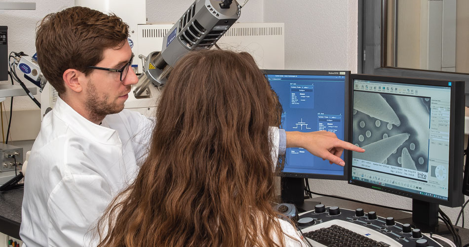
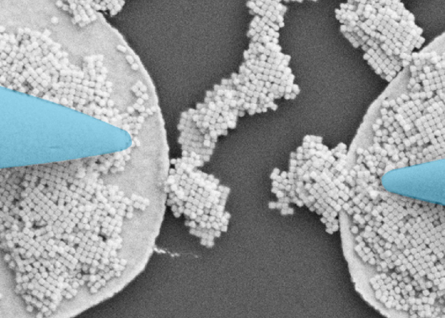
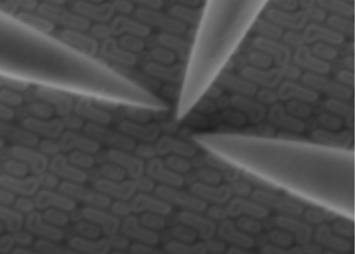
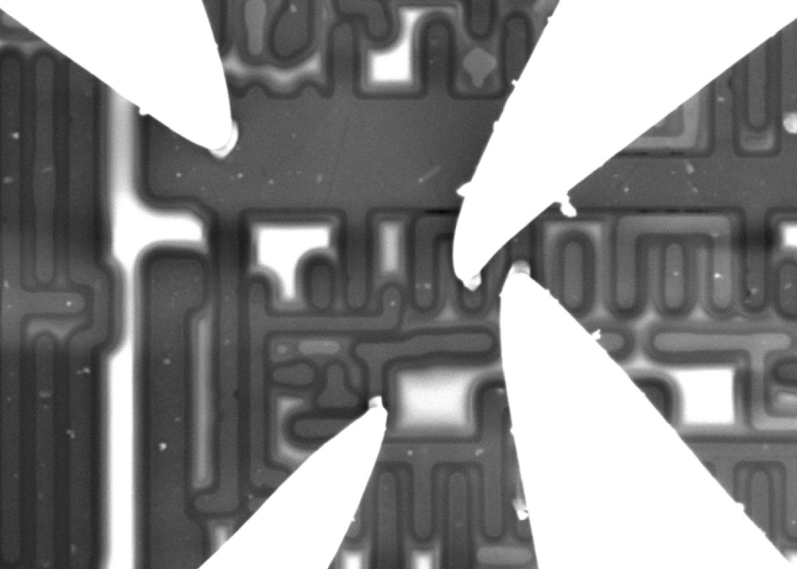
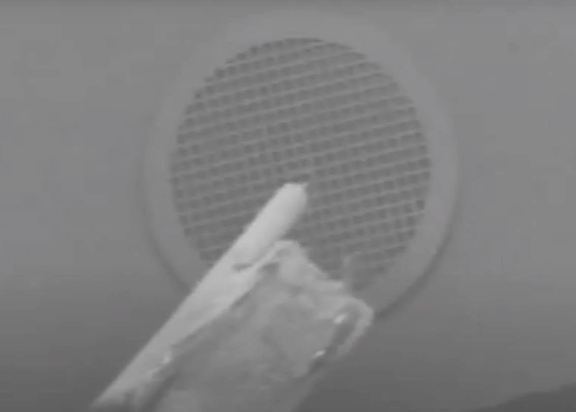
Jump to Navigation
Home
  • Contact us
  • Home
  • Products
  • Applications
  • Events
  • Company

Search form

Electron Microscopy (SEM/FIB)

Imina Technologies nanomanipulation platforms are compatible with a wide range of scanning electron microscope vacuum chambers. In situ electrical and mechanical characterization of new materials is made easy by using several miBot nanomanipulators with different probes and sensors. Learn more about our turnkey solutions.

Bending of Nanowires

Materials Science

Calculate the Young's modulus of a nanowire.

TEM Sample Preparation

Materials Science

Deposition of an 80 nm nanowire on TEM grid inside a Scanning Electron Microscope (SEM).

AFM Probe Tip Decoration

Materials Science

Nanoparticles manipulation and assembly.

MEMS / NEMS Testing

Electronics

Deformation of an AFM cantilever observed at the SEM.

Nanowires Manipulation

Materials Science

in situ characterization of nanowires inside a SEM.

  • All
  • Electron Microscopy (SEM/FIB)
  • Optical Microscopy

Download product brochure

  • Home
  • Products
    • Our solutions
    • Platforms for Optical & Electron Microscopes
    • Components
    • Micro & Nanomanipulator
    • Standard Platform Base
    • Compact Base
    • Piezoelectric Amplifier
    • User Interface
    • Options
    • Positioning Stage
    • Electrical Probing
    • Probes & Micro-Tools
  • Applications
    • All
    • Electron Microscopy (SEM/FIB)
    • Optical Microscopy
  • Events
    • Next Conferences & Fairs
    • Past Events
  • Company
    • About us
    • Awards
    • Company news
    • Contact
    • Sales inquiry
    • Directions
  • Contact us

Subscribe to our newsletter

  • Follow us on Twitter
  • Visit our Facebook page
  • Watch videos on our YouTube channel
  • Subscribe to our news feed
  • Read the latest news about science
Legal Notice | © 2012 Imina Technologies. All rights reserved.