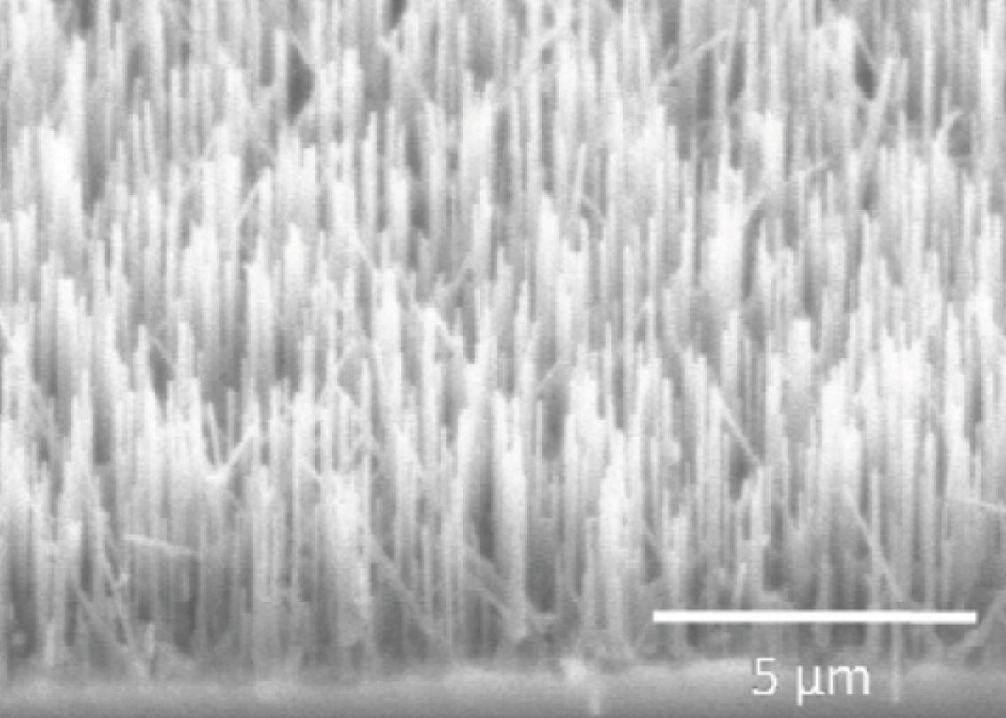
Semiconductivity and photoconductivity have, among other properties of nanowires, potential applications in the next generation of electronic and photonic devices such as transistors, solar cells, LEDs and detectors. In order to be able one day to utilize these unique properties, further characterization of single nanowires is still needed.
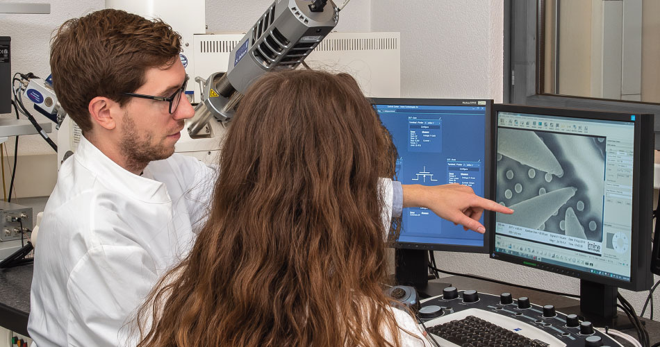
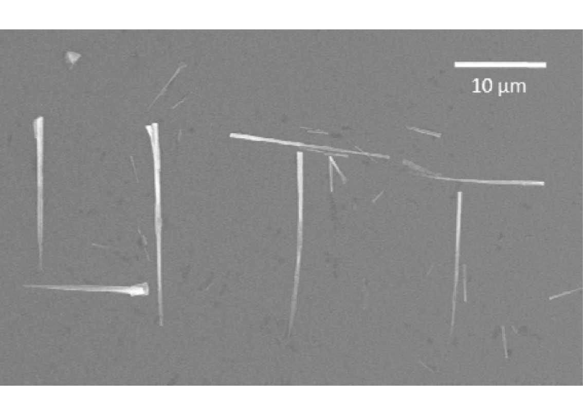
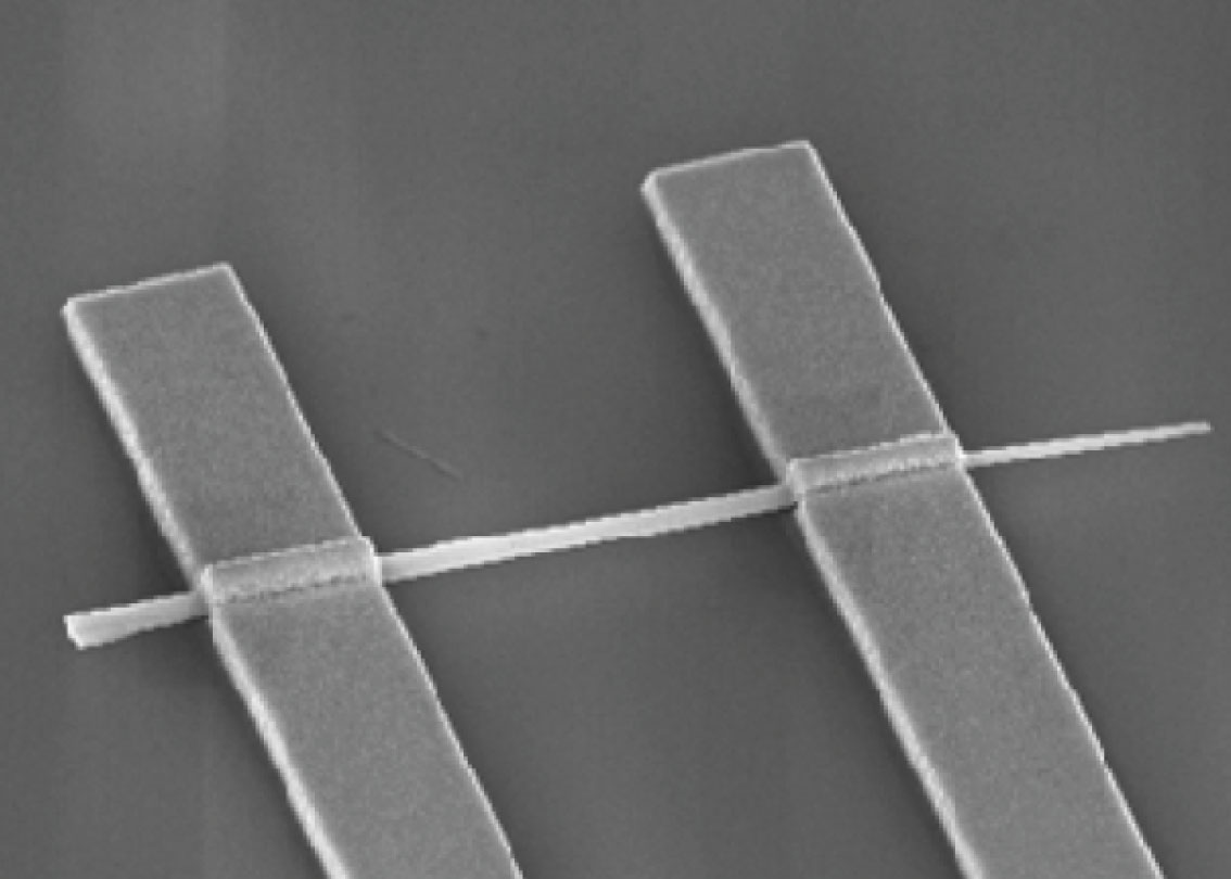
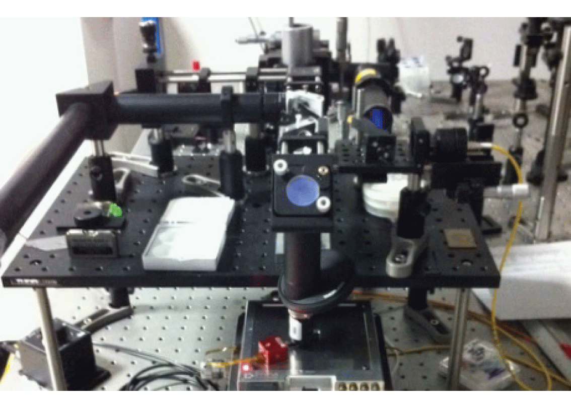
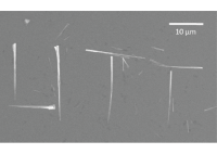
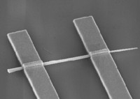
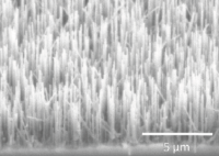
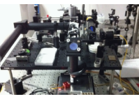
This application note reports on the use of Imina Technologies miBot manipulators to carry out the delicate step that consists in positioning the nanowires grown by metalorganic chemical vapour deposition (MOCVD) at specific locations on the substrate.
Geng, W., Kostcheev, S., Sartel, C., Sallet, V., Molinari, M., Simonetti, O., Lérondel, G., Giraudet, L. and Couteau, C. (2013), Ohmic contact on single ZnO nanowires grown by MOCVD, Phys. Status Solidi C, 10: 1292–1296.
We have fully equipped demo lab for semiconductor electrical failure analysis. Our applications team is eager to perform live demonstrations and feasibility studies for you, onsite or online.
In the meantime, do not miss the opportunity to learn more about our products and applications with one of our webinars!