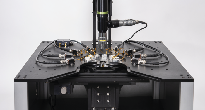
The miBot micromanipulators used in conjunction with an adequate XYZ positioning stage and optics offer a unique combination of flexibility and automation capabilities for wafer testing. The compact design of the miBot makes it a very stable prober to position probe tips with sub-micron resolution over centimeter range.
Controlled from a personal computer via either an intuitive software GUI or a control pad, the probes can easily be placed in contact with pads and lines and quickly adapt to different samples.
Automated testing procedures can be used to accelerate data acquisition when measures have to be repeated several times at different locations on the wafer, for instance in a wafer-level failure analysis process.
This video illustrates an automated sequence in which two miBot are operated to electrically contact micron size pads. The process is configured and run from Precio™, Imina Technologies' software suite.
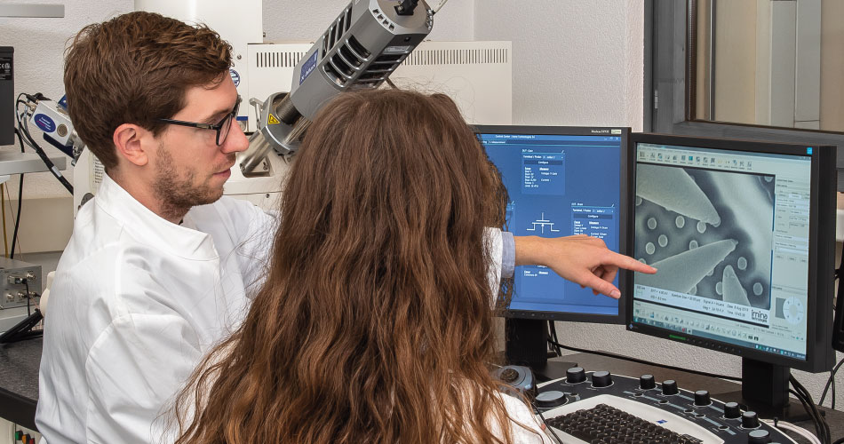
We have fully equipped demo lab for semiconductor electrical failure analysis. Our applications team is eager to perform live demonstrations and feasibility studies for you, onsite or online.
In the meantime, do not miss the opportunity to learn more about our products and applications with one of our webinars!