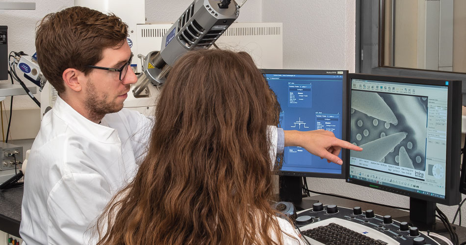
Some components of MEMS devices are less than a few hundred microns in size. It becomes difficult to access electrical contacts or other components on such scale.
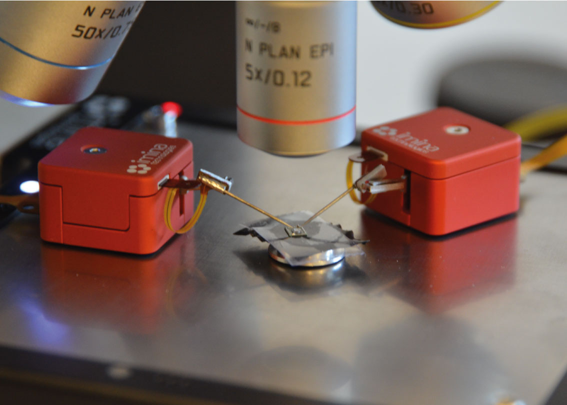
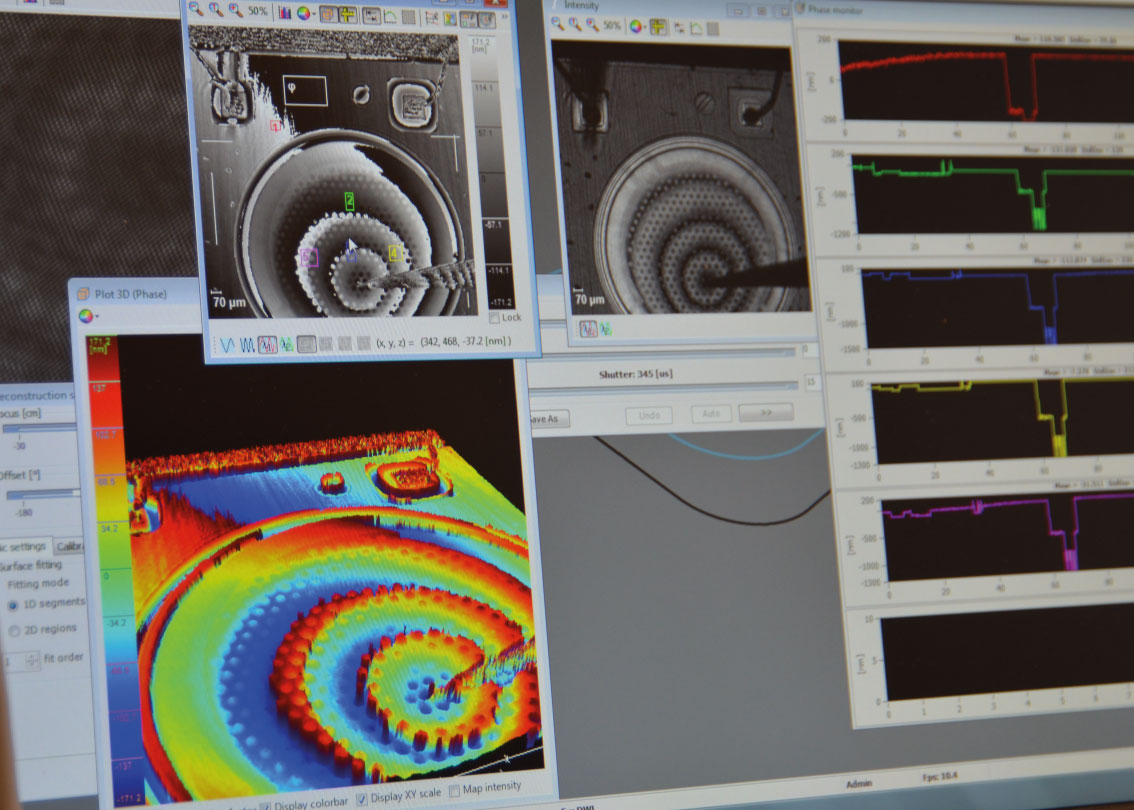
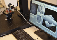
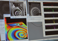
In this application note, we show how two miBot micromanipulators with tungsten probes can actuate to an electrothermal MEMS resonator. The silicon membrane of the MEMS device is then characterized with Digital Holographic Microscopy (DHM) to determine its resonant frequencies and image its deformation.
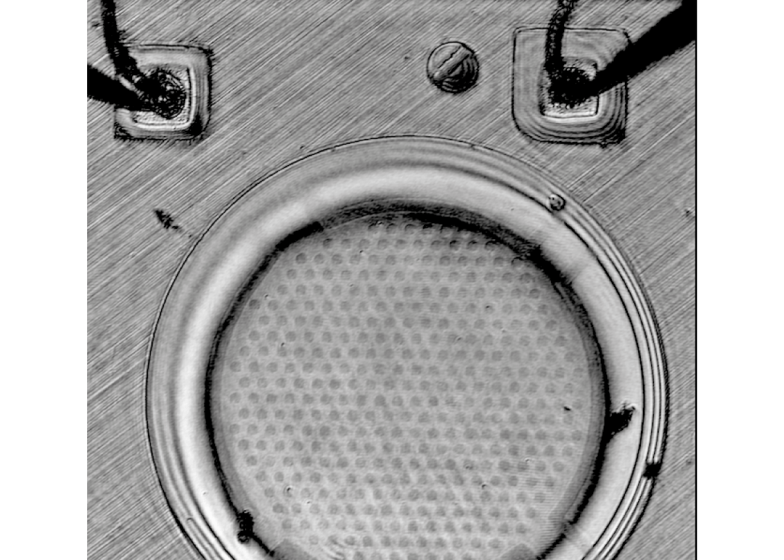
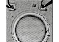
Also pictured from the same experiment, is a miBot probe used to mechanically deform the silicon membrane of the MEMS resonator, which was dome on the same sample and setup.
We have fully equipped demo lab for semiconductor electrical failure analysis. Our applications team is eager to perform live demonstrations and feasibility studies for you, onsite or online.
In the meantime, do not miss the opportunity to learn more about our products and applications with one of our webinars!