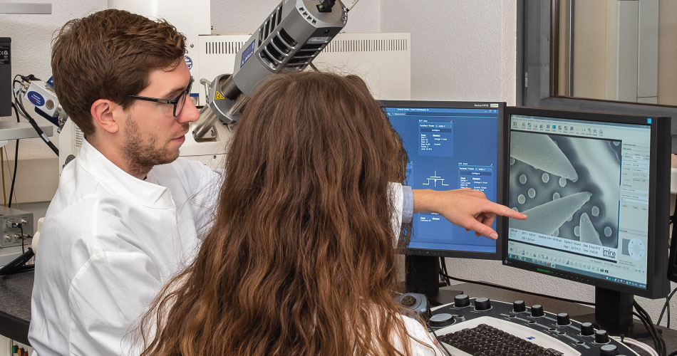
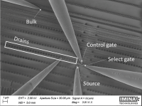
Electrical nanoprobing of non-functional bits is challenging for several reasons. Such measurements require landing 5 probes and maintaining them in contact. A tricky task, especially when working in high-resolution imaging conditions (short working distance, low kV). On top of that, lengthy exposure to e-beam can affect the bits, for example by erasing a written bit.
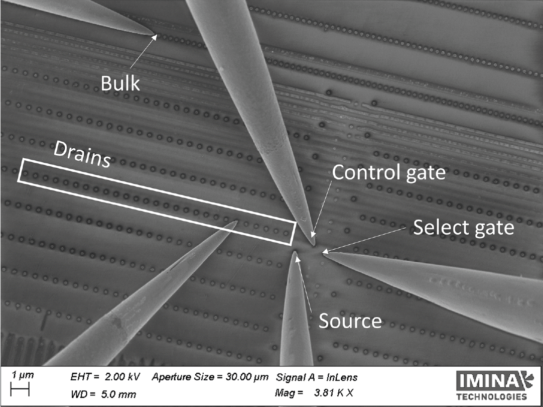
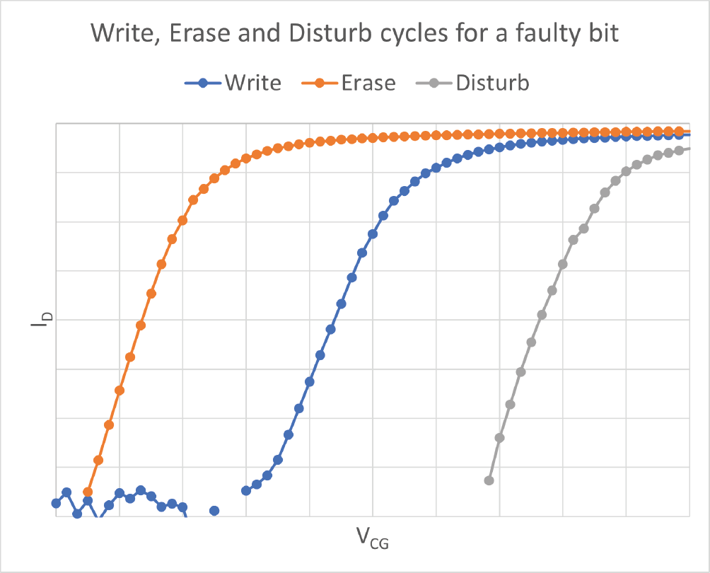
We characterized a known faulty bit and compared its behavior with a functional one in the same memory array. We found that the faulty bit changed its value after several operations on other bits around it. Further measurements showed that in the faulty bit, the leakage current between the Drain and the Bulk was several orders of magnitude higher than that in the functional one.
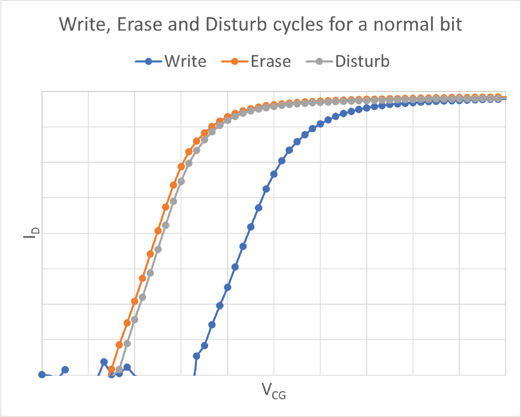
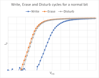
We have also studied e-beam effects on functional bits. After a few minutes’ exposure to the 2kV electron beam, the bit value was erased.
Transistor characterization of a 5nm SRAM die
Femtofarad capacitance-voltage measurement at transistor contact level
We have fully equipped demo lab for semiconductor electrical failure analysis. Our applications team is eager to perform live demonstrations and feasibility studies for you, onsite or online.
In the meantime, do not miss the opportunity to learn more about our products and applications with one of our webinars!