Capacitance-Voltage measurements are an important tool to characterize the gate oxide in detail. They provide information about dopant concentration profile, input and output capacitance of the transistor, gate oxide thickness, dopant density, flat-band voltage, gate oxide quality, and interface charge.
When the gate capacitance of the transistor in question is in femtoFarad (fF) range, such measurements can be affected by noise, offsets, etc.
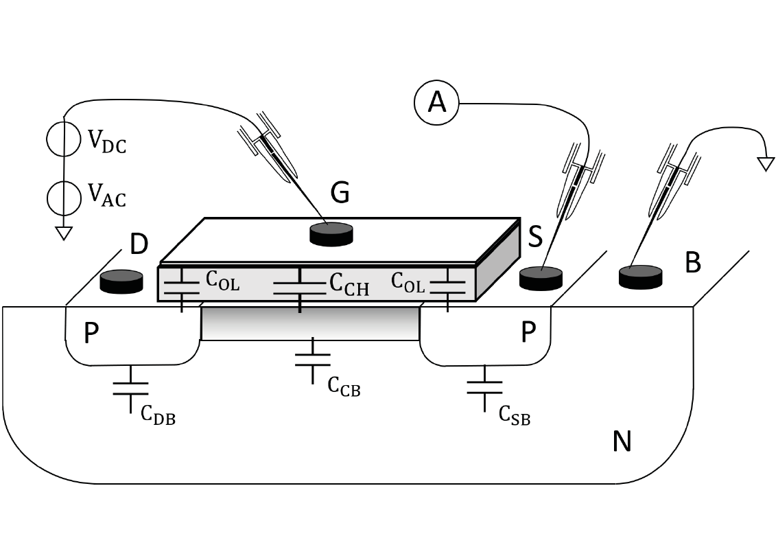
In this application note, we discuss how to measure fF-scale gate capacitance of a MOSFET exposed at the contact level using our Nanoprobing Solution and a semiconductor parameter analyzer Keithley 4200A-SCS.
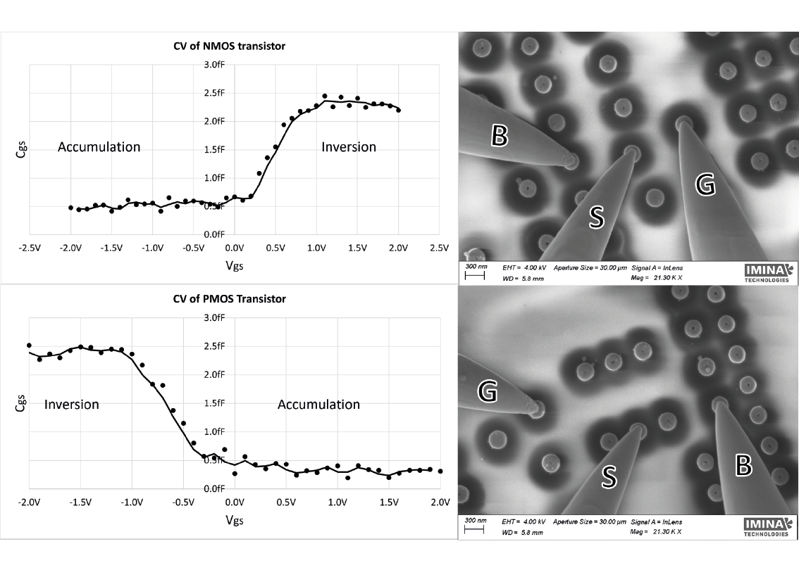
We demonstrate low-noise measurements of capacitances down to 2.5fF with the noise around 50 aF. We can measure such low capacitance thanks to 1) Imina Technologies’ probers being robust against noise; 2) Careful wiring of the Keithley CV Unit.
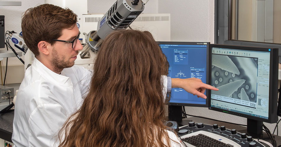
Electrical nanoprobing on 22, 14, and 10 nm semiconductor devices
We have fully equipped demo lab for semiconductor electrical failure analysis. Our applications team is eager to perform live demonstrations and feasibility studies for you, onsite or online.
In the meantime, do not miss the opportunity to learn more about our products and applications with one of our webinars!