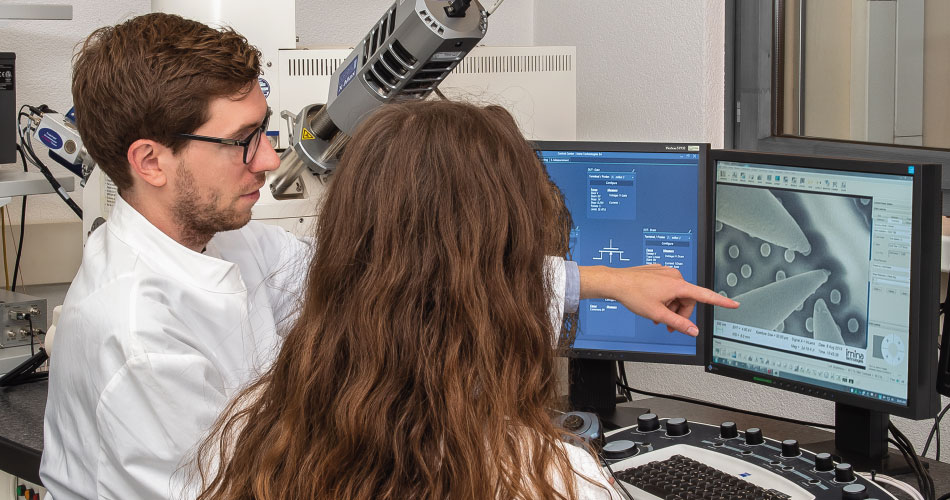
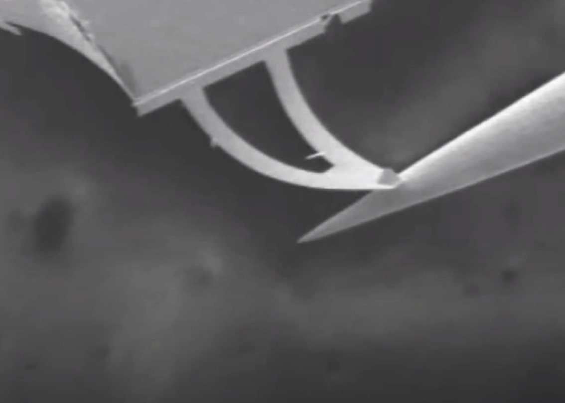
Reliability and fatigue tests need to be carried out on new MEMS / NEMS devices to validate motions of new designs. In situ tests in SEM or under optical microscope are often preferred during the R&D phase so that abnormalities or defects can be rapidly detected. This video features a miBot used to deform an AFM cantilever while it is observed at the SEM.
We have fully equipped demo lab for semiconductor electrical failure analysis. Our applications team is eager to perform live demonstrations and feasibility studies for you, onsite or online.
In the meantime, do not miss the opportunity to learn more about our products and applications with one of our webinars!