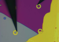
2D materials such as graphene and transitional metal dichalcogenides are very promising as building blocks for efficient and compact photovoltaic devices. Active layers made of 2D materials can have a total thickness of a few nanometers, making ultrathin devices possible.
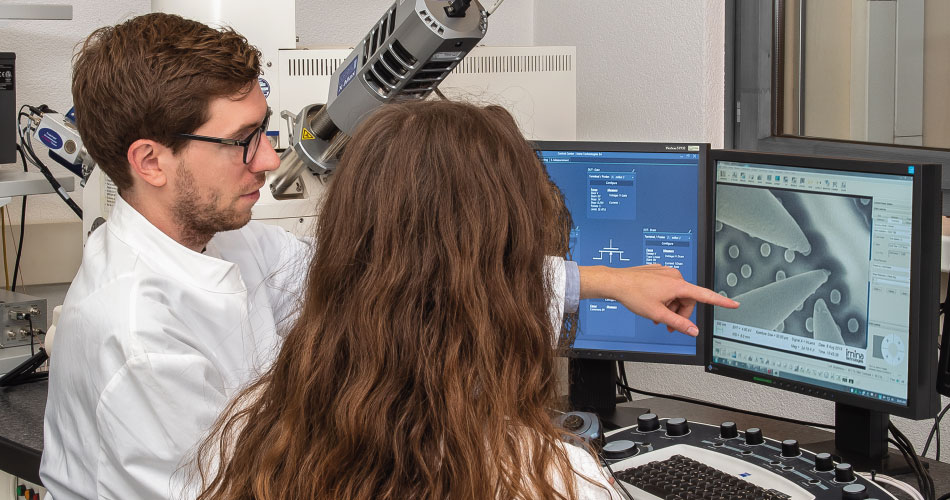
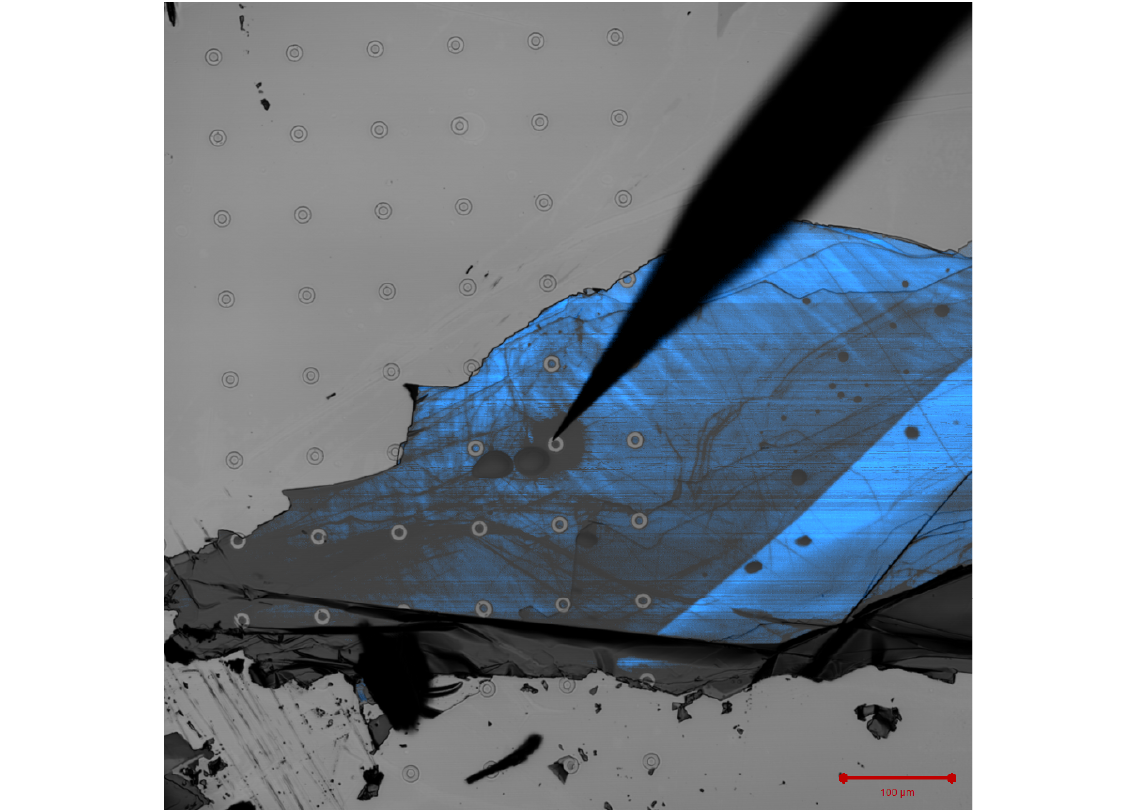
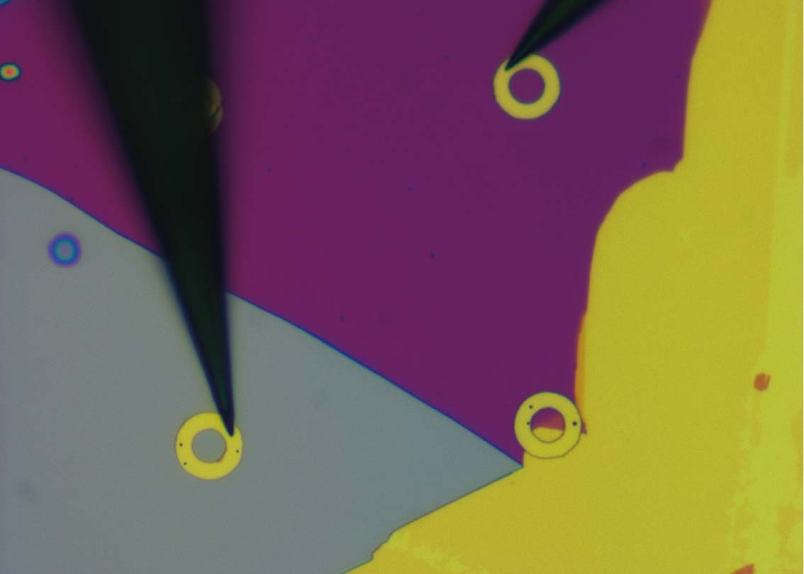
Characterization of such devices is challenging because it requires extremely gentle electrical contact to avoid damaging the thin layers. Safe and straightforward probe landing is an essential feature of Imina Technologies’ MICRO probe stations. All our MICRO solutions combine nanoscale precision of piezo-controlled motion with an intuitive user interface for gentle and safe probe landing on fragile samples.
"miBots are an invaluable tool for nanoscience research in our group. We rely on them for making electrical contacts to various optoelectronic samples," says Joeson Wong, an active IMINA user at the Atwater Research Group in Caltech.
Atwater Research Group, Caltech
Deep Jariwala, Artur R. Davoyan, Giulia Tagliabue, Michelle C. Sherrott, Joeson Wong, and Harry A. Atwater, Near-Unity Absorption in van der Waals Semiconductors for Ultrathin Optoelectronics, Nano Letters, 2016 16 (9), 5482-5487
Joeson Wong, Deep Jariwala, Giulia Tagliabue, Kevin Tat, Artur R. Davoyan, Michelle C. Sherrott, and Harry A. Atwater, High Photovoltaic Quantum Efficiency in Ultrathin van der Waals Heterostructures, ACS Nano, 2017 11 (7), 7230-7240
Cora M. Went, Joeson Wong, Phillip R. Jahelka, Michael Kelzenberg, Souvik Biswas, Matthew S. Hunt, Abigail Carbone and Harry A. Atwater, A new metal transfer process for van der Waals contacts to vertical Schottky-junction transition metal dichalcogenide photovoltaics, Science Advances, 7, 44, (2021)
We have fully equipped demo lab for semiconductor electrical failure analysis. Our applications team is eager to perform live demonstrations and feasibility studies for you, onsite or online.
In the meantime, do not miss the opportunity to learn more about our products and applications with one of our webinars!