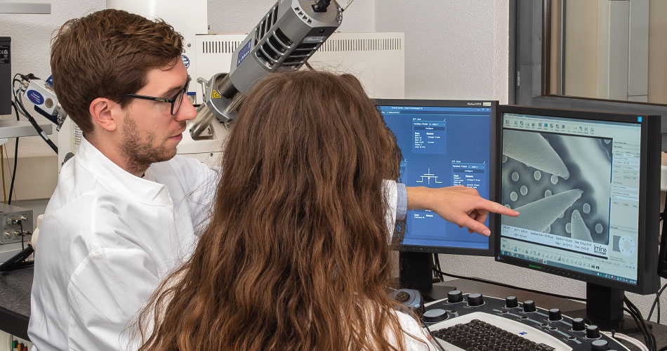
NEMS resonators based on nanowires have many applications as resonators and switches. In order to characterize pull-in and resonator properties of these devices, the strength of clamping when a bending force is applied has to be evaluated. However, when the nanowire being tested is only a hundred nanometers wide and a few micrometers in length, it is difficult to apply a displacement with the required positioning and motion resolutions.
In this experiment, under SEM, a miBot nanomanipulator with a 500 nm tungsten probe is used to displace single-crystal silicon nanowires (SiNW) 194 nm in diameter and 50 µm in length at the middle of the wires, while the ends are clamped. The SiNWs are slowly displaced until fracture occurs either at the clamping points or elsewhere in the wires to determine the clamping or fracture strengths, respectively. This is acquired by observing the displacements just before failure in SEM then using this data with a large-scale displacement model in COMSOL to determine the fracture strengths.
Microelectronic Systems Laboratory, EPFL, Lausanne, Switzerland
Evren F Arkan, Davide Sacchetto, Izzet Yildiz, Yusuf Leblebici and B Erdem Alaca, Monolithic Integration of Si Nanowires with Metallic Electrodes: NEMS Resonator and Switch Applications, December 2011, J. Micromech. Microeng. 21 125018.
We have fully equipped demo lab for semiconductor electrical failure analysis. Our applications team is eager to perform live demonstrations and feasibility studies for you, onsite or online.
In the meantime, do not miss the opportunity to learn more about our products and applications with one of our webinars!
