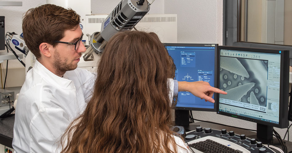
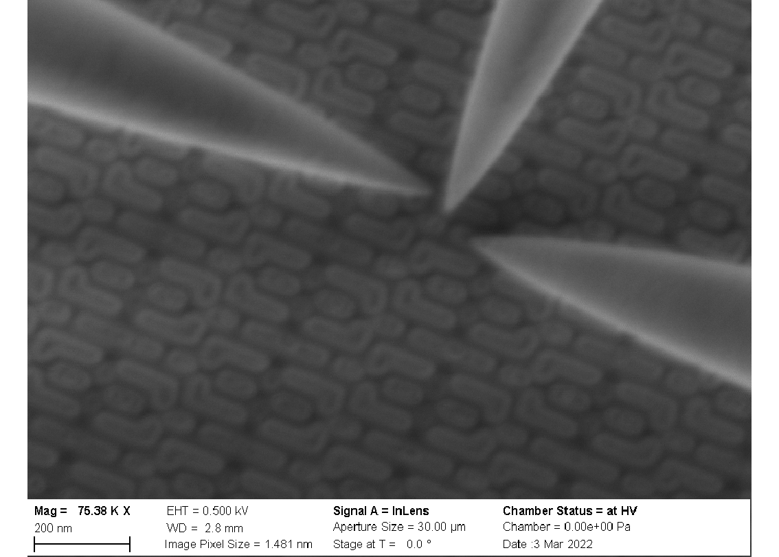
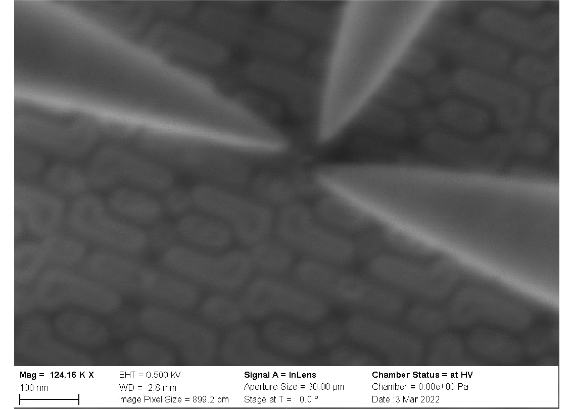
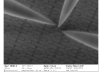
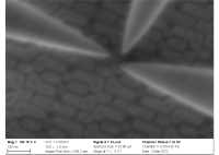
Nanoprobing of small technology-node devices can be very time-consuming. To navigate around the sample and to contact the device under test, one has to operate the SEM under low acceleration voltage and short working distance. These imaging conditions result in comparatively poor image contrast, slowing the operator down.
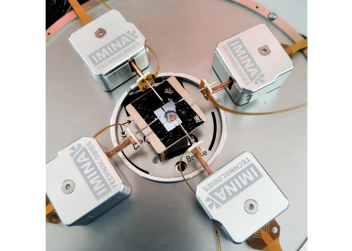
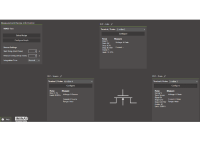
Sample Positioning XYZ Sub-Stage significantly speeds up the process. It helps to quickly move from one ROI to another without having to move the probers one by one. It also helps to approach or to retract the sample to/from the probers much faster.
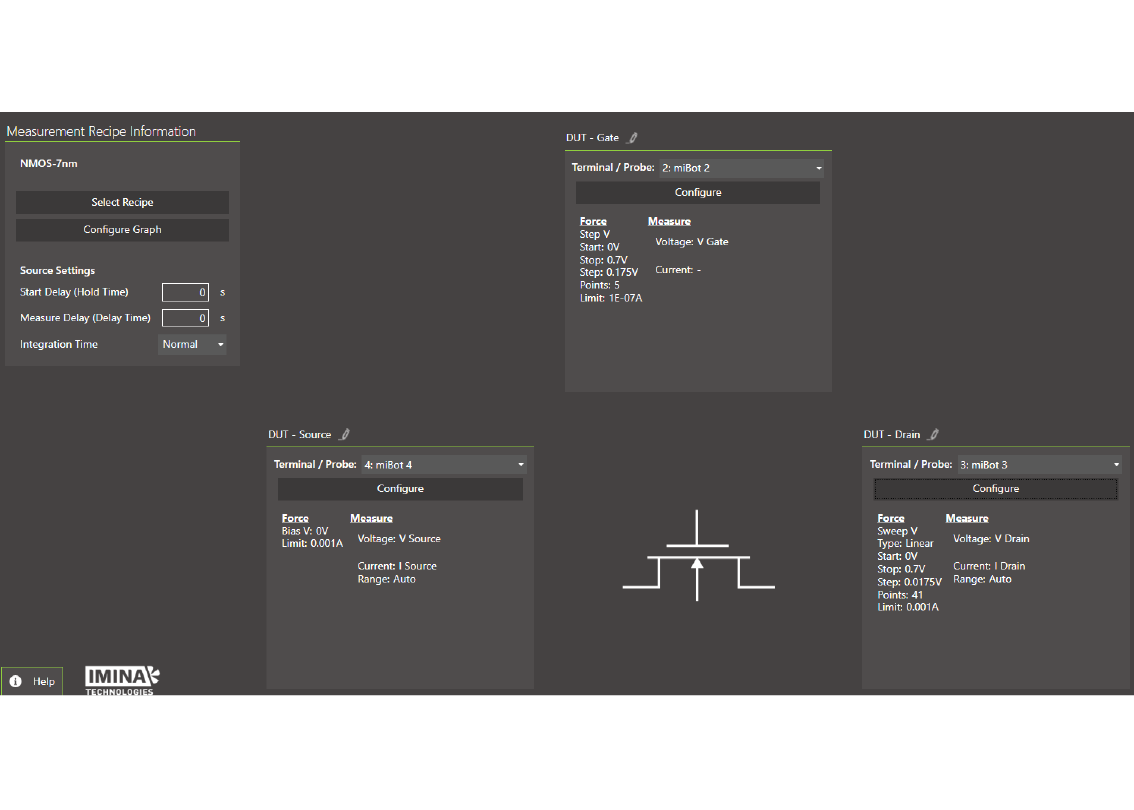
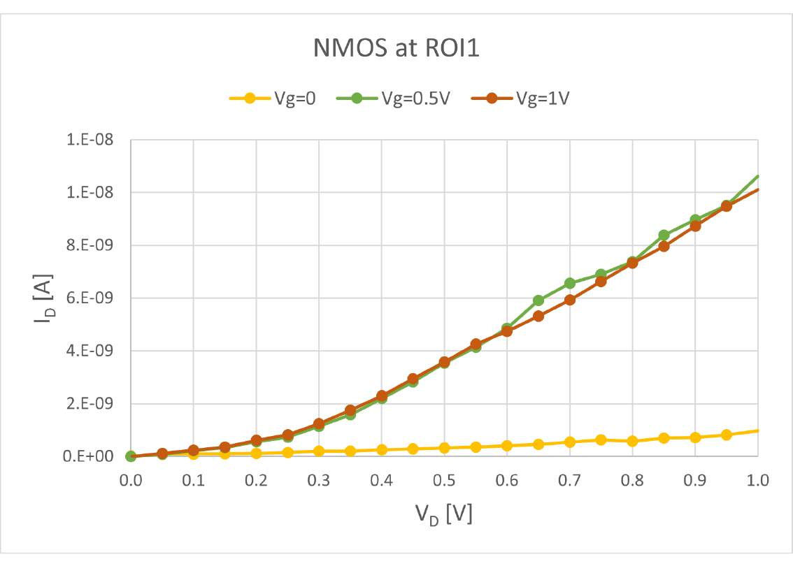
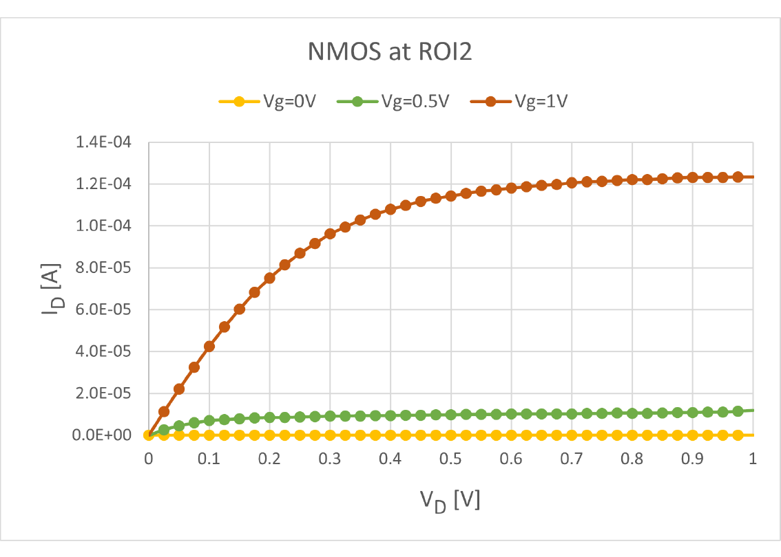
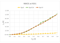
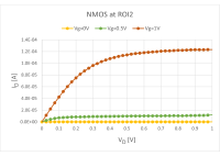
We show that with the Sample Positioning XYZ Sub-Stage, the characterization of NMOS transistors of a 7 nm semiconductor technology nodes is three times faster than without the Sub-Stage.
Transistor characterization of a 5nm SRAM die
Failure mechanism investigation of single bits in flash memory array
We have fully equipped demo lab for semiconductor electrical failure analysis. Our applications team is eager to perform live demonstrations and feasibility studies for you, onsite or online.
In the meantime, do not miss the opportunity to learn more about our products and applications with one of our webinars!