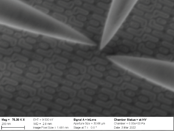
Components of integrated circuits are constantly shrinking in size. To keep up with this trend, IC design and electrical failure analysis engineers rely on nanoprobing in scanning electron microscope (SEM) to characterize the performance of microchips.
Read our new application note to learn about advantages of using Imina Technologies’ Nanoprobing Solution for characterization of NMOS and PMOS transistors of a 7 nm technology node chip.