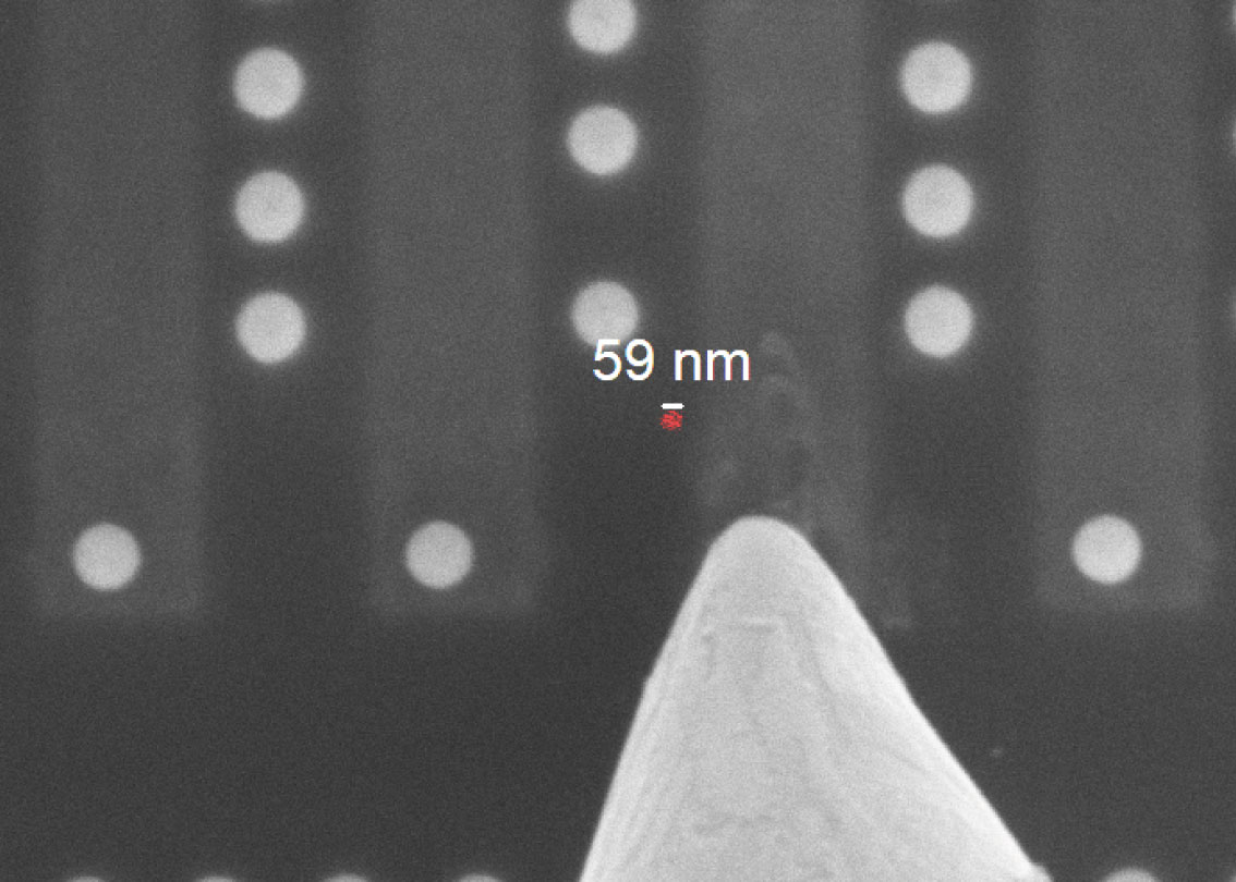
Together with Dialog Semiconductor and Point Electronic, Imina Technologies presents a new use case of its nanoprobing solution for semiconductor defect localization using the Electron Beam Induced Resistance Change (EBIRCh) technique.
Results are presented in a detailed application note, describing the use of this technique to accurately localize a defect in the gate oxide of a transistor. The high stability and positioning resolution of our nanoprobing solution combined with Point Electronic’s highly sensitive electrical failure analysis system made this experiment a success.
Feel free to contact our applications team for more information or to book your personal demonstration. And to explore more use cases, please visit our applications webpage.