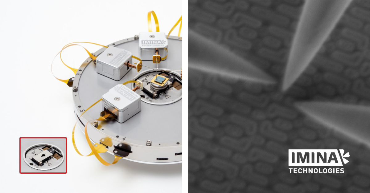
Characterization of small tech node transistors is a time-consuming task. We found a way to significantly speed up the workflow so the user can focus on the most delicate procedures such as final landing probes and easily probe different regions of the sample.
Our Sample Positioning XYZ Sub-Stage allows the user to move the sample laterally or vertically independently from the probes. In our new application note, we show a three-fold speed-up in characterization of the 7 nm SRAM transistors, as compared to the experiments without the sub-stage. It is used to find the most suitable sample area for characterization.
You can also watch the Sub-Stage in action, where it is used to characterize multiple 65 nm node transistors.