News

April, 2023

miBots used in combination with EFA techniques at KIST

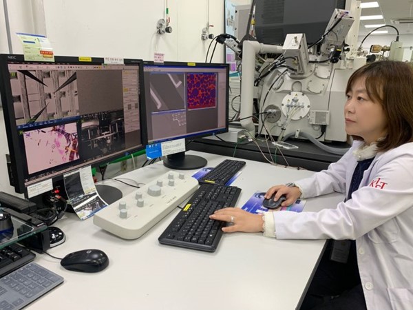
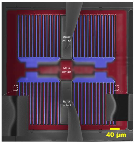
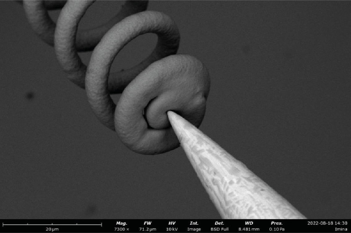
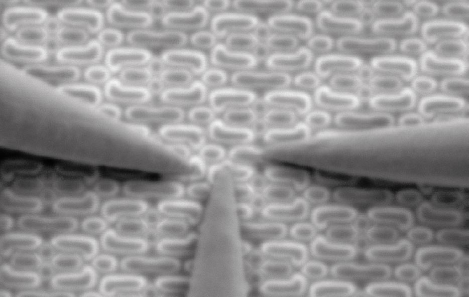
Nanoprobing combined with EBIC/EBAC helps to reveal charge carrier dynamics in perovskite solar cell and to study electrical conductivity in battery materials.
March, 2023

miBots used to actuate MEMS

SEM imaging used to detect sub-100 nm or high-frequency in-plane MEMS motion.
March, 2023

Partnership with Eurofins MASER

Imina Technologies and Eurofins MASER join forces to offer top-level service in Nanoprobing and Electrical Failure Analysis.
February, 2023

The In-situ Microscopy Alliance

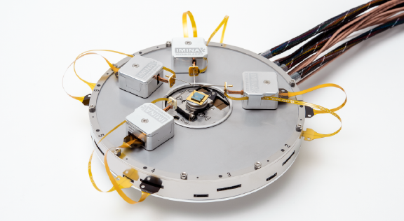
Alemnis, Imina Technologies, NenoVision and point electronic form an alliance to jointly provide in-situ characterization tools, solutions and services.
February, 2023

Speed up in situ SEM electrical nanoprobing

Threefold speed-up in the characterization of 7 nm transistors using a substage.
February, 2023

Manipulation and probing in a desktop SEM

Quick and precise microprobing inside a desktop SEM now available.
January, 2023

New distributor in the UK and Ireland

Scanwel Ltd is now our exclusive distributor in the UK and Ireland.
December, 2022

5nm transistor characterization

New application note about electrical nanoprobing of NMOS and PMOS transistors of a 5 nm technology node chip.
August, 2022

New distributor in Israel

Picotech appointed as exclusive distributor for Imina Technologies’ product in Israel.
July, 2022

New demo lab in Singapore at WinTech Nano

Top in-situ SEM nanoprobing and electrical failure analysis system is now available in Singapore at WinTech Nano for demonstrations and services.