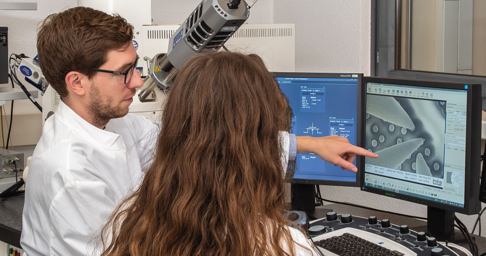
Integrated nanoprobing solutions for your SEM, FIB and dual beam.
Perform electrical characterization of microelectronic devices, in situ semiconductor failure analysis and manipulation of single structures under electron microscopes.
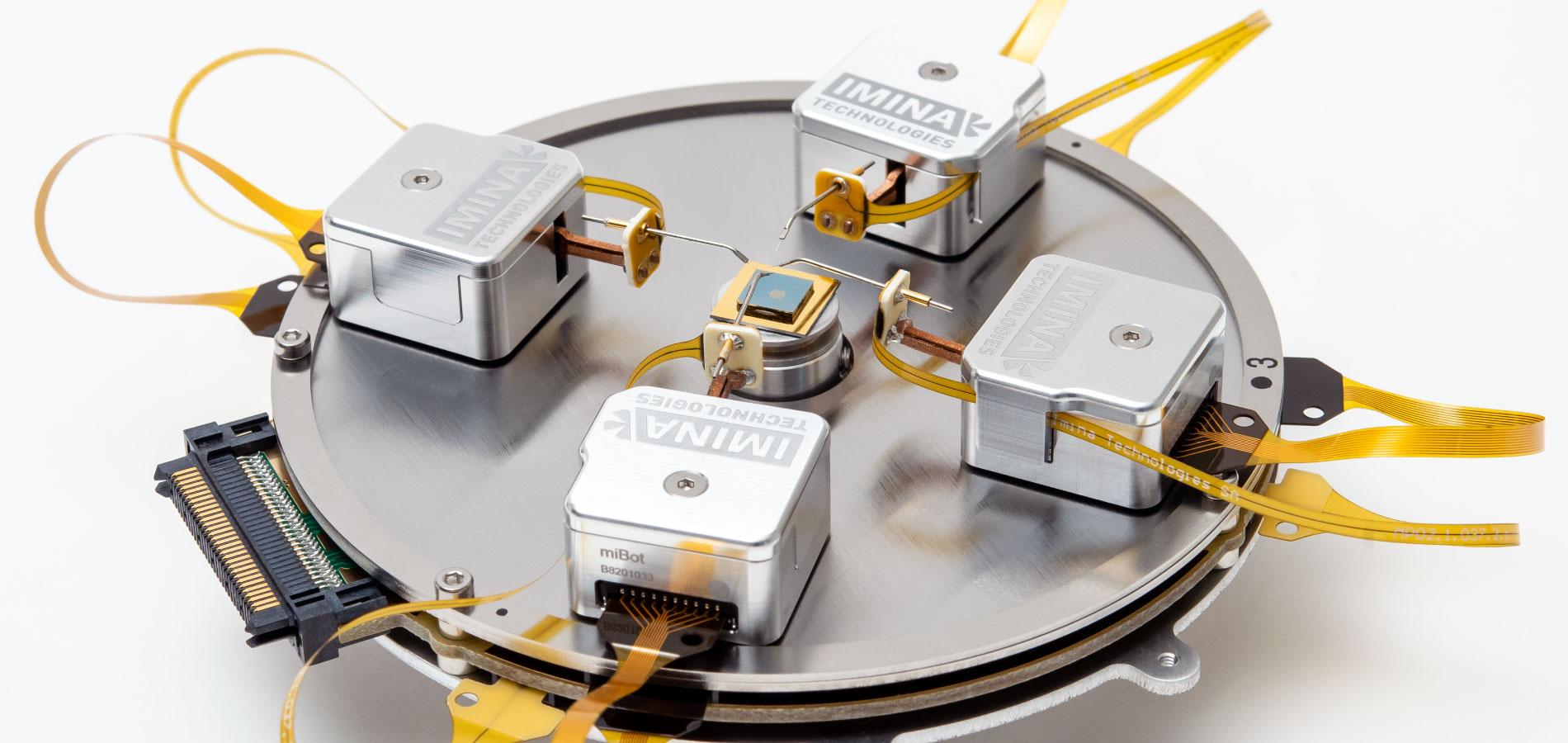
Integrated nanoprobing solutions for your SEM, FIB and dual beam.
Perform electrical characterization of microelectronic devices, in situ semiconductor failure analysis and manipulation of single structures under electron microscopes.
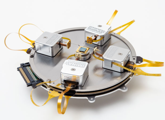
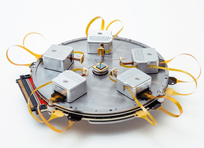
Up to 8 miBot™ nanoprobers can be delivered in various configurations and options to adapt to your specific application requirements and microscopy equipment. The compact and light platforms for the robots are compatible with any electron microscope and can either be mounted on the SEM sample positioning stage, or be loaded via the SEM load-lock.
Designed to match the most demanding technical and operational requirements of the semiconductor industry, our nanoprobing solutions integrate smoothly within standard FA workflows and feature numerous benefits to reduce the time to data.
Gain agility to solve your challenges! Our solutions offer unmatched flexibility for straight forward adaptation to changes of experimental setups and specimens. In no time they can adapt to different sample sizes and geometries.
Modify your nanoprobing setup by adding or removing robots to the platform. Adjust their position and orientation, by hand before closing the microscope door, or remotely when in situ.
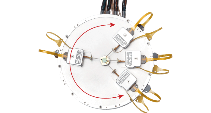
The compatibility with high resolution imaging using magnetic lenses enables the operator to perform nanoprobing experiments with the most advanced scanning electron microscopes on the market and take advantage of the highest resolution imaging capabilities, even at accelerating voltages below 0.5 kV. And as the whole platform and robots can be tilted, in situ FIB circuit editing and nanoprobing can be performed simultaneously providing faster and more accurate failure analysis results.
| Magnetic immersion mode
|
Tilted angles
|
Short working distances
|
 |
 |
 |
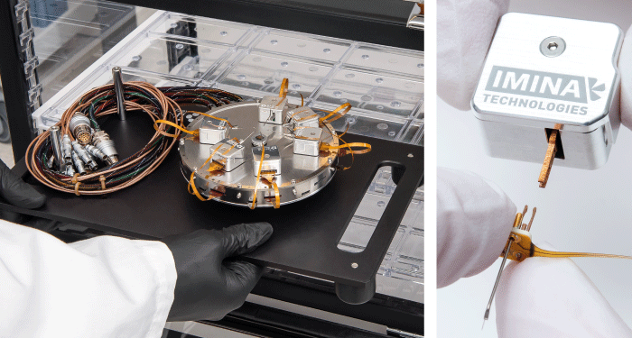
No permanent modification of the microscope chamber is required and the installation and removal of the system only takes a few minutes. This avoids having to dedicate an SEM for nanoprobing and makes it possible to quickly transfer the system from one microscope to another (additional SEM integration kits available in option) or store it in our compact contamination-free storing solution.
Industry standard electrical probes are safely mounted on the nanoprobers and replaced in minutes thanks to our patented probe holder.
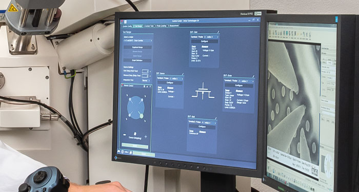
Our solutions are fully controlled from Precisio™ software suite, a unified and intuitive application, providing a step by step operator assistance to position the nanoprobes, run and process electrical test measurements:
Configure the NANO solution just the way you need it to match the requirements of your application, types of samples, and microscope. Don’t know what to choose? No worries, let us assist you.
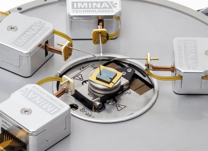
Move the sample independently from the probes in X, Y, Z directions with nm resolution. Reduce probes landing time and accelerate multiple devices characterization.
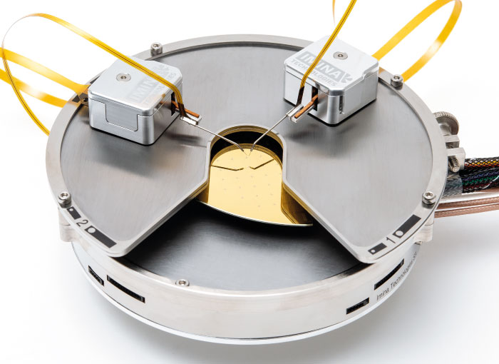
This adapter gets mounted with a single screw on the nanoprobing stage. It raises the miBot robots and provide space below for large and packaged samples.
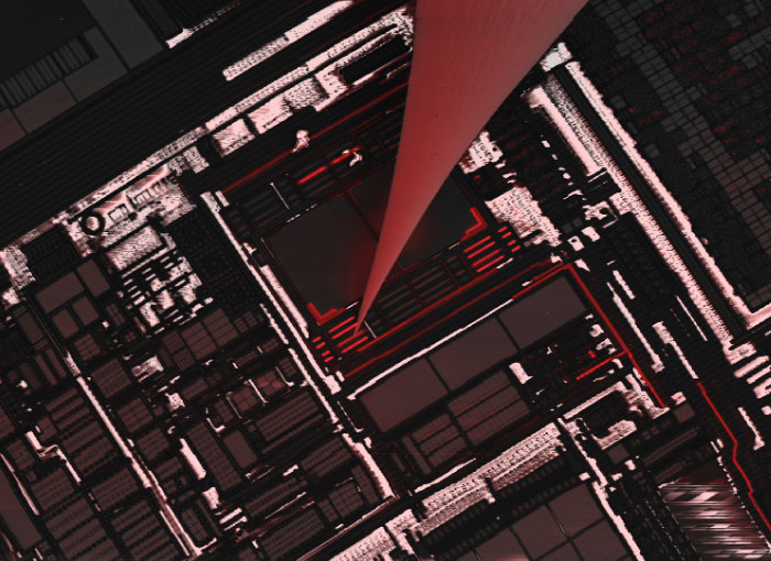
High performance and integrated quantitative system for Electrical Failure Analysis (EFA) in SEM and Dual-Beam, including EBAC/RCI, EBIC, EBIRCh and related techniques.
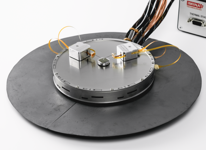
Vibration-free thermal stage for precise temperature control in the range from -30°C to 150°C. Flexible radiator can be folded to fit the thermal stage into small SEM chambers.
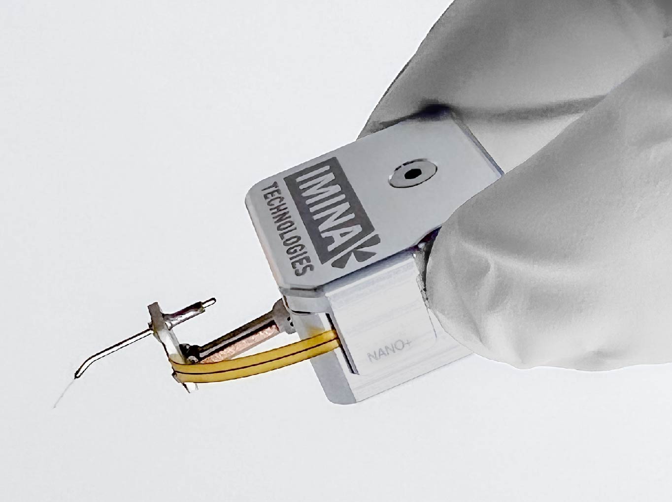
2-4 times faster and safer probe landing thanks to the fine-mode (scanning) motion of the piezo actuator in Z axis extended to 15 µm. Available as an upgrade.
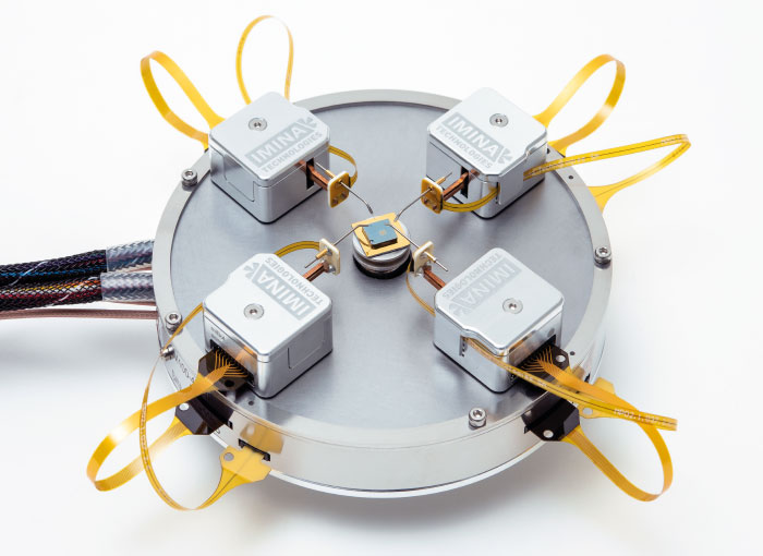
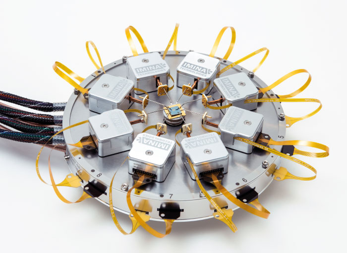
Would you like to integrate our nanoprobing solutions in non-conventional vacuum chambers or with third party analytical equipment?
Feel free to contact us, we have solutions for integration with:
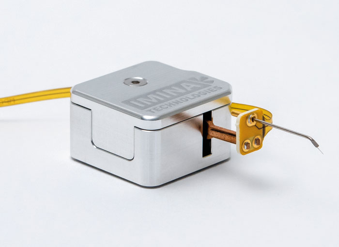
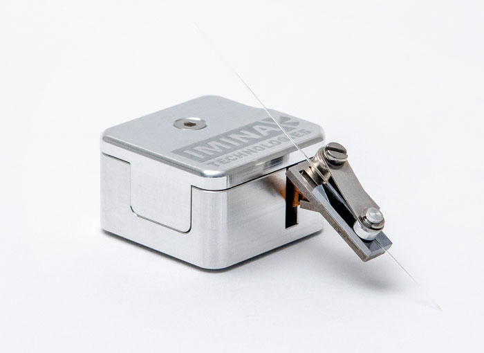
The exchange of tools is fast and convenient with the miBot’s patented tool holder mechanism. In minutes, turn the miBot from an electric probe or optical fiber positioner into a manipulator of nanoparticles or biological samples. Do you need to position other tools like for example a MEMS, multiprobes, miniforks, AFM probes, or force sensors?
Contact us, several OEM tools holders are available upon request
| Nanoprober miBot™ NANO | 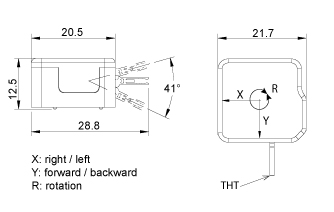 |
|
| Degrees of freedom | 4 independently driven (X,Y,R,Z) per prober | |
| Dimensions & weight | Body: 20.5 x 21.7 x 12.5 mm3
Arm: 8.3 mm (without tool) Weight: 12 g (without tool) |
|
| Max. positioning resolution | Motion modes: coarse (stepping) and fine (scanning)
Stepping: 60 nm (X, Y), 120 nm (Z) Scanning: 0.02 nm (X, Y), 0.1 nm (Z) |
|
| Motion range | Stepping (XY,R,Z): 20 x 20 mm2 , ± 180°, 41°
Scanning (X Y Z): 250 x 440 x 780 nm3 Note: in stepping, actual X, Y, R range are only limited by the size and shape of the stage where the miBot moves, and the length of the driving cable. |
|
| Speed | X and Y: up to 1.5 mm.s-1 Z: up to 150 mrad.s-1
|
|
| Forces & torques | X and Y: push: 0.3 N Z: lift: 0.7 mNm (5 g)
hold: 0.2 N hold: 0.9 mNm (6 g) |
|
| Tilt angle | Holding position up to 55°
|
|
| Drift
|
< 1 nm/min
|
|
| Tool holders | Range of holders for probes and optical fibers
|
|
| Specifications are measured at tool-holder tip (label “THT” on schema) and measured at 300 K with motion controller MC410/20 and robot BT-19. | ||
| Electrical probing
|
|
| Voltage range
|
± 100V
|
| Current range
|
100 mA
|
| Leakage current
|
<100 fA/V
|
| Bandwidth
|
Max. 25 MHz
|
| Resistance
|
Approx. 3.5 Ω from probe tip to flange connectors
|
| Low noise probing accessories and suitable measurement environments are required to achieve the best measurement performance of the system
|
|
We have a fully equipped demo lab for semiconductor electrical failure analysis. Our applications team is eager to perform live demonstrations and feasibility studies for you, onsite or online.
In the meantime, do not miss the opportunity to learn more about our products and applications with one of our webinars!
