High-electron mobility transistors (HEMTs) are important components for high-power and high-frequency applications. Thousands of hours of HEMT operation can result in a non-homogenous current distribution due to the heating effects. To ensure reliable long-term operation, HEMTs design should be optimized accounting for what is known about their failure mechanisms.
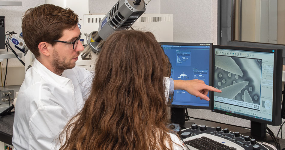
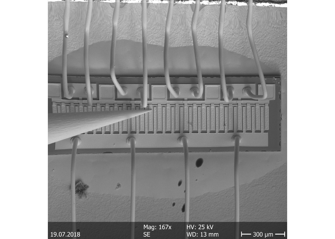
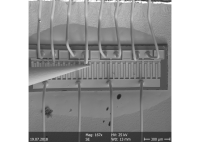
Researchers from the Materials Physics Group (GPM) in Rouen, France, study AlGaN/GaN HEMTs. For in-situ electrical failure analysis, the group relies on Imina Technologies' NANO setup with the EFA option. The combined setup is used for electron beam induced current (EBIC) measurements. Other failure analysis techniques complement EBIC to test the feasibility of AlGaN/GaN technology and to understand the failure mechanisms in more detail.
“It took us only two training sessions to master nanoprobing and EBIC. It is quite easy to land probes on components surfaces and get the EBIC data.” – says Prof. Olivier Latry, who is leading this study.
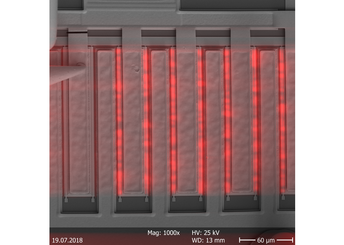
In their recent work, researchers confirmed that the temperature effects are more important in the center of a die than on the edges, which is consistent with infra-red measurements. Based on this knowledge, they can now optimize the heating regulation, find a better substrate and a base plate, etc.
“We use EBIC to understand the correlation between the produced current and what happens on the component: threshold voltage, non-uniformity, damaged p-n junction, etc. EBIC is very helpful in comparing the same family of components. We use the setup mainly on GaN HEMTs but also on SiC MOSFETs.”
Materials Physics Group (GPM), University of Rouen
N. Moultif, S. Duguay, O. Latry, M. Ndiaye, E. Joubert, Reliability and failure analysis in power GaN-HEMTs during S-band pulsed-RF operating, Microelectronics Reliability, Volume 126, November 2021, 114295
Electrical failure analysis and semiconductor defect localization techniques
We have fully equipped demo lab for semiconductor electrical failure analysis. Our applications team is eager to perform live demonstrations and feasibility studies for you, onsite or online.
In the meantime, do not miss the opportunity to learn more about our products and applications with one of our webinars!