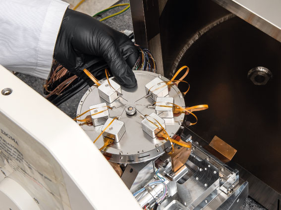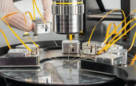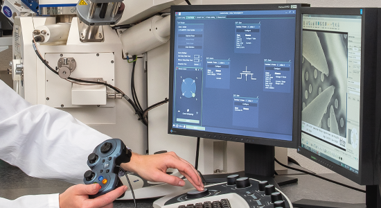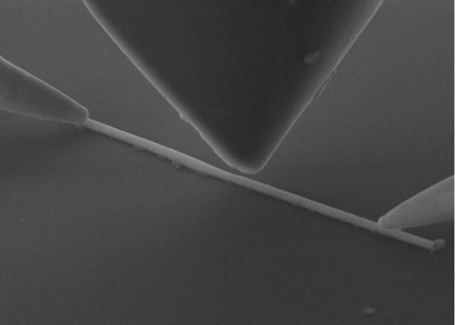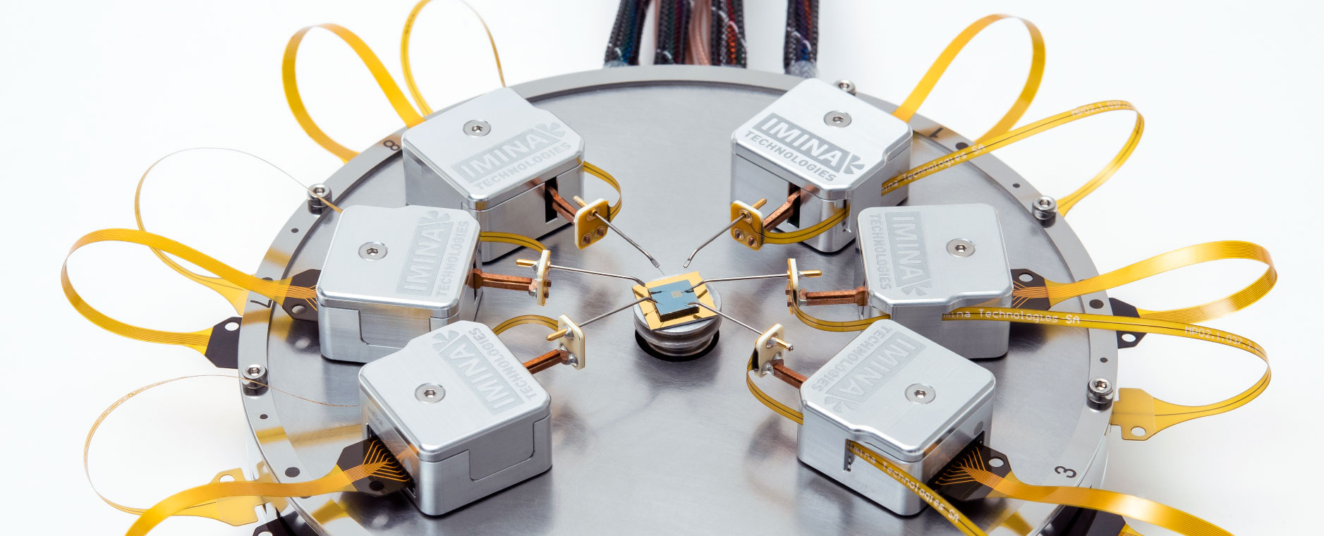
We offer high-precision robotic solutions to interact with and characterize samples down to the nanometer scale. Based on a unique motion technology, positioning probes with our robots and maintaining stable electrical contacts has never been so easy. The high modularity of our solutions provides considerable flexibility for deep integration with a variety of microscopy and test equipment, enabling efficient measurement workflows.
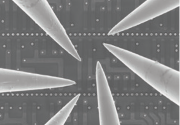
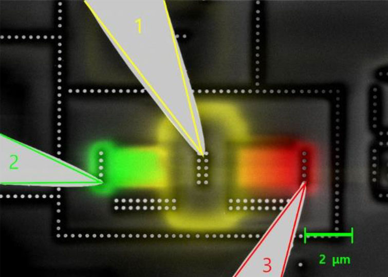
 Electrical Probing
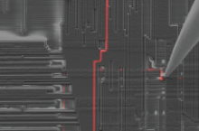
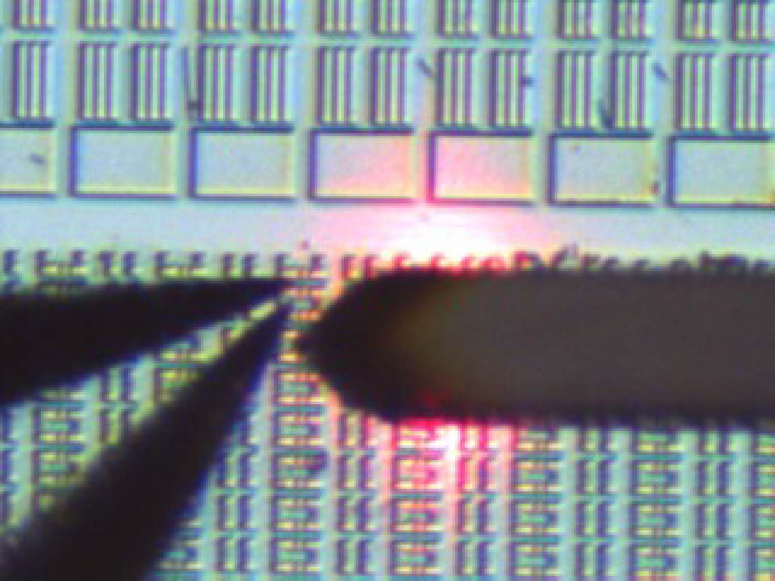
 Failure Analysis
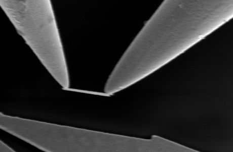
 Manipulation