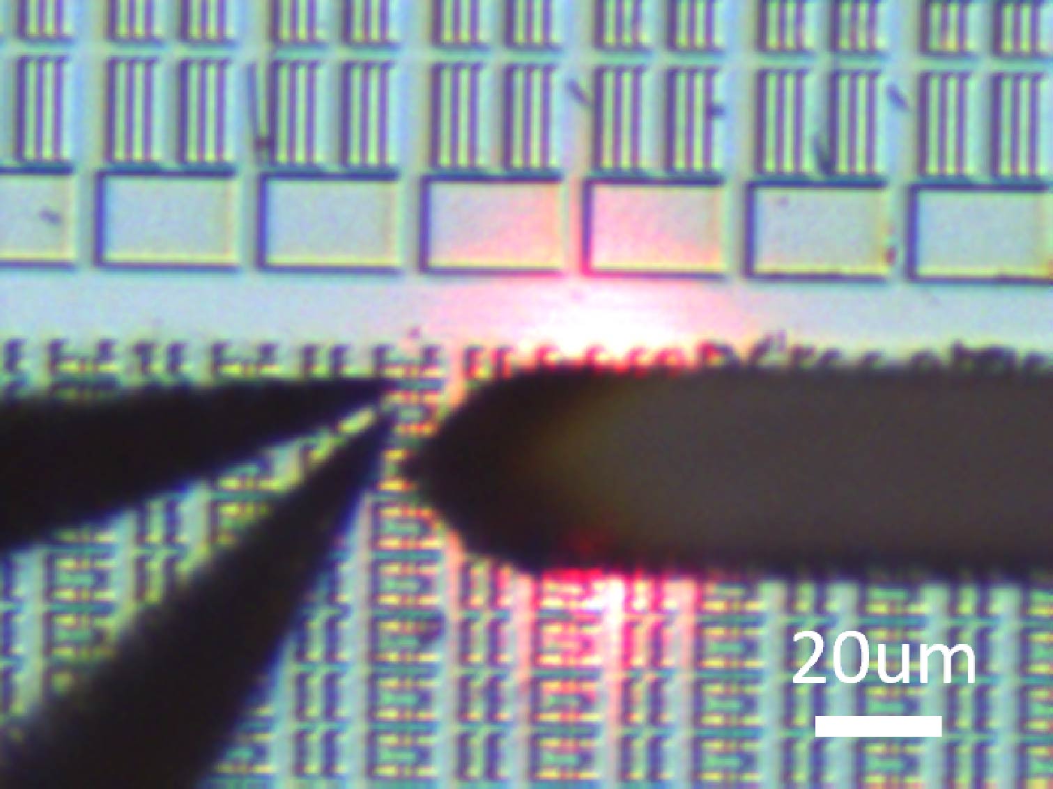
Together with Bruker, we have integrated miBots™ into Atomic Force Microscopy (AFM) for simultaneous AFM and electrical probing. Such setup opens access to complex analysis of various materials and in-situ AFM of operating or actuated devices. miBots can be added to existing Dimension Icon setups. They are easy to install, use, and can be integrated into other analytical tools (optical microscopes, etc).
Bruker Dimension Icon™ AFM was chosen for this integration as its tip holder has a large clearance, so miBots™ fit on the sample stage and leave sufficient room for the AFM tip. Thanks to Bruker Dimension Icon’s ‘scan-by-tip’ design, miBots can be integrated without compromising scanning quality and speed. With miBots’ compact build, it is easy and safe to land the probes next to the AFM tip.
Electrical nanoprobing is compatible with different advanced AFM-based characterization modes, such as Electric Field Microscopy (EFM), Kelvin Probe Force Microscopy (KPFM), Magnetic Force Microscopy (MFM), Piezoresponse Force Microscopy (PFM), Conductive-AFM, Tunneling-AFM (TUNA), Scanning Capacitance Microscopy (SCM), Scanning Spreading Resistance Microscopy (SSRM), Scanning Thermal Microscopy (SThM), to name a few.
To illustrate the power of the combined approach, we ran Kelvin Probe Force Microscopy (KPFM) experiments on various metallic structures and semiconductor devices in operating conditions. Read our application note to learn more.