Applications

Filter by:
Microscope
Technique
Domain
Nanomanipulation of individual nanowires using electrostatic forces in-situ SEM
Electron Manipulation Materials Science

In situ nanomanipulation in SEM

Manipulation of a single Gd-doped ceria (MIEC) nanofiber inside SEM to prepare for TEM electrochemical measurements.
Electron Manipulation Materials Science

Manipulation of MIEC nanofibers

Semi-automated robotic manipulation of micron-scale biological samples with end-effectors under an optical microscope.
Optical Manipulation Materials Science

Robots cooperation for microparticles manipulation

Nanometer-scale manipulations on nanowires with nanoprobers in a SEM and a TEM.
Electron Manipulation Materials Science

TEM sample preparation

Precise positioning of an optical fiber to measure the spectral characteristics of a light-emitting diode.
Optical Manipulation Photonics

Fiber optic positionning

Organic piezoresistive U-shaped microcantilevers used as MEMS, optimal composite material selected based on performance.
Optical Manipulation Electronics

Electromechanical characterization of MEMS

Observation under a SEM to monitor the deformation of an AFM cantiveler. A miBot is employed to deform the AFM.
Electron Manipulation Electronics

MEMS / NEMS mechanical testing

Nanoprober tip pushinga a sub-200 nm-diameter, 50-micrometer-long single-crystal silicon nanowire resonator to fracture.
Electron Manipulation Probing Electronics

Characterization of SiNW based NEMS resonator

Ohmic contacts on ZnO nanowire fabricated by e-beam lithography on individual wires prepositioned in-situ by nano probes.
Optical Manipulation Electronics Photonics

Nanowires micromanipulation

miBots holding a optical fiber to illuminate the solar cell locally and contacting it to measure the electrical response.
Optical Manipulation Probing Photonics

Photovoltaic characterization of PV solar cells

Microgrippers and microprobes move Barium Titanate microparticles with a diameter ranging from 10 to 30 micrometers.
Optical Manipulation Materials Science

Micro-particles manipulation and sorting

Because seeing is believing!

We have fully equipped demo lab for semiconductor electrical failure analysis. Our applications team is eager to perform live demonstrations and feasibility studies for you, onsite or online.

Book your demo today!

In the meantime, do not miss the opportunity to learn more about our products and applications with one of our webinars!
Register to a webinar

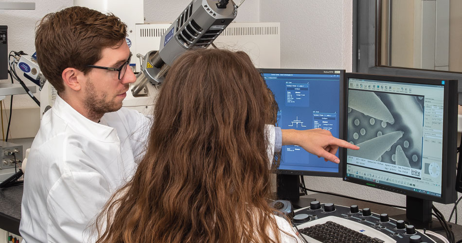
Imina Technologies' application engineer shows a colleague how to land probes on nanoscale contacts for in-situ SEM transistor characterization.