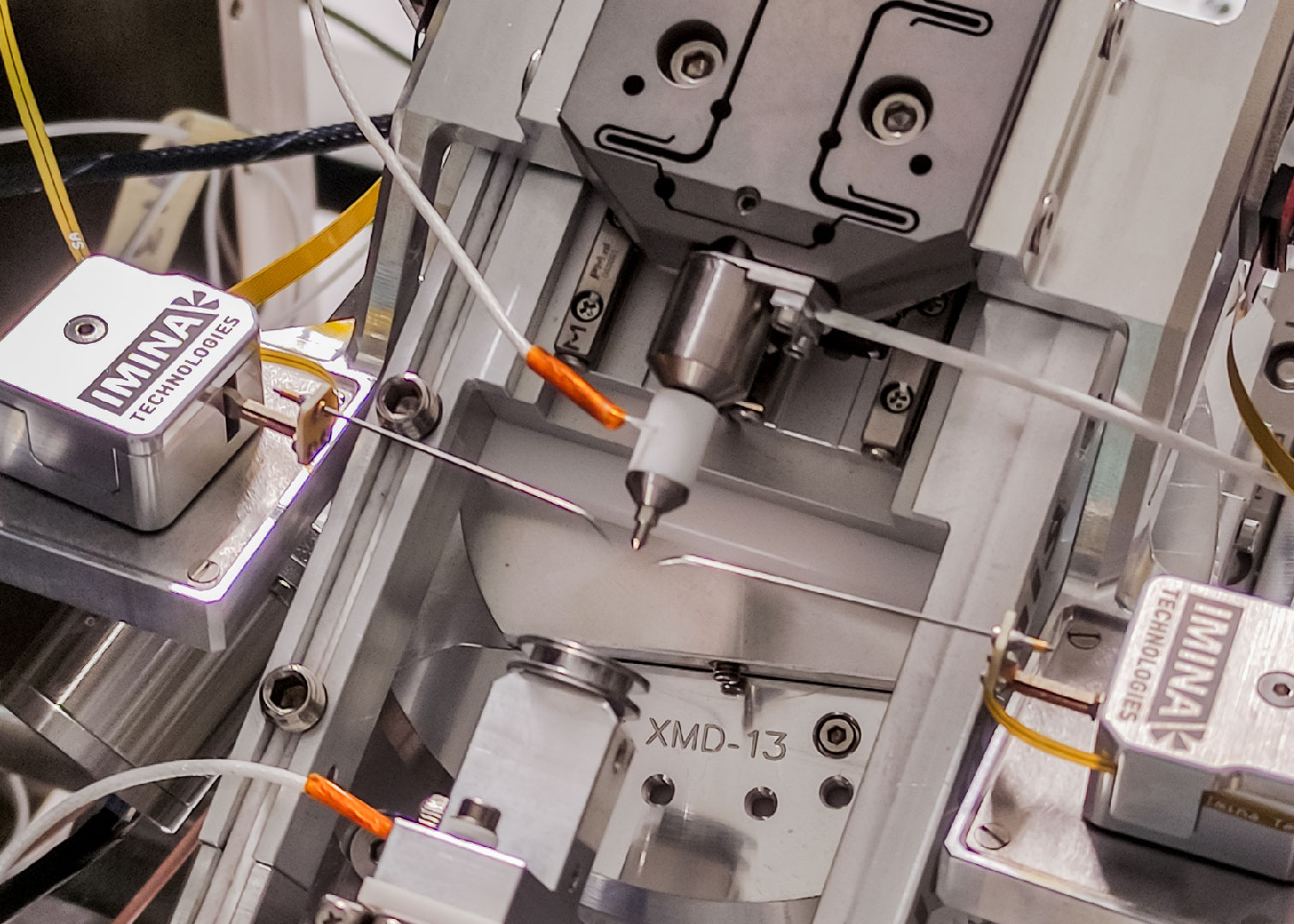
We are happy to present to you an integrated solution for simultaneous nanoprobing and nanoindentation inside the SEM. This solution was developed together with another Swiss high-precision instrumentation company, Alemnis, who is one of our In-Situ Microscopy Alliance partners.
Simultaneous electrical nanoprobing and nanoindentation can yield microscale insights into how mechanical pressure and deformation affect electrical properties of different materials and devices. This integrated solution will take the experiments aiming to understand the microscale phenomena to the next level and will help design safer semiconductor devices.
This integrated solution is straightforward to use, easy to learn and comes as a turnkey product with support from both companies.
To demonstrate the capabilities of our integrated solution, we studied the deformation of an actuated piezoresistive AFM cantilever and the change of electrical current passing through a deformed PtCr metal line. Learn more from our application note.