Electrical nano probing combined with nanoindentation inside SEM can elucidate the effects of mechanical pressure and deformation on electrical properties on the smallest scales. And other way round, such setup can be used to study a displacement caused by an electrical bias or actuation, for example, in MEMS or NEMS.
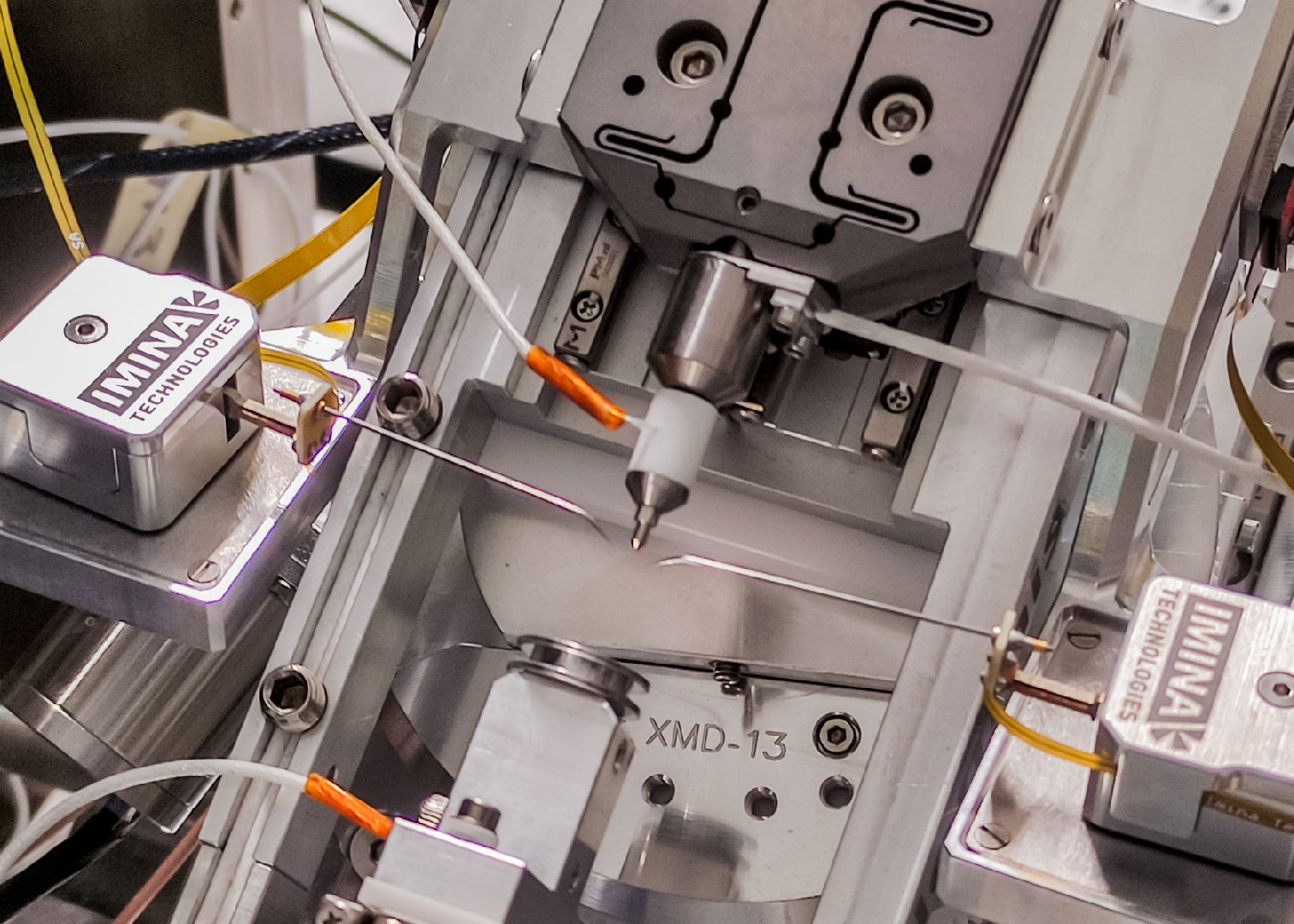
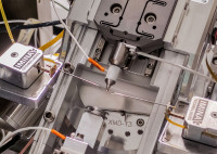
Two Swiss high-precision instrumentation companies, Imina Technologies and Alemnis, now offer an integrated solution for simultaneous nanoprobing and nanoindentation inside the SEM.
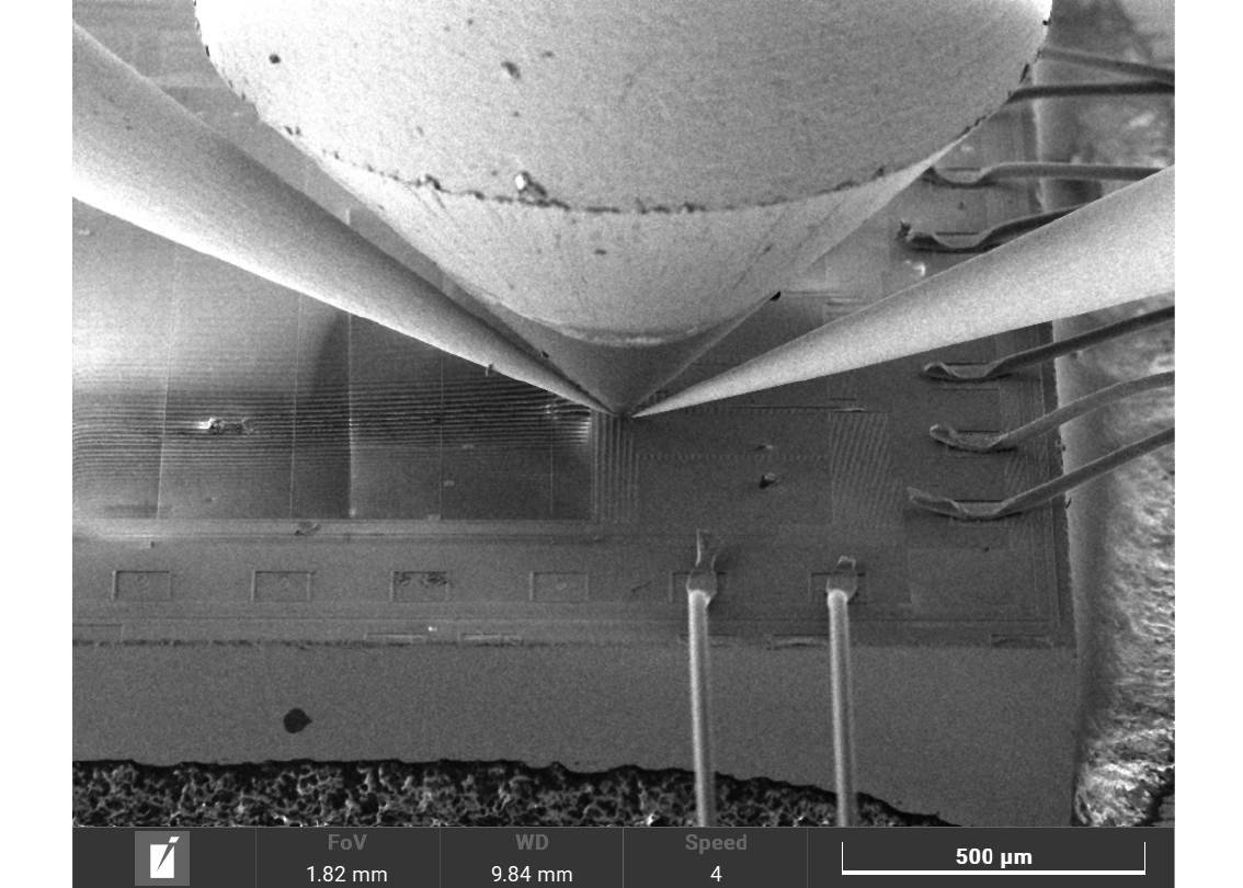
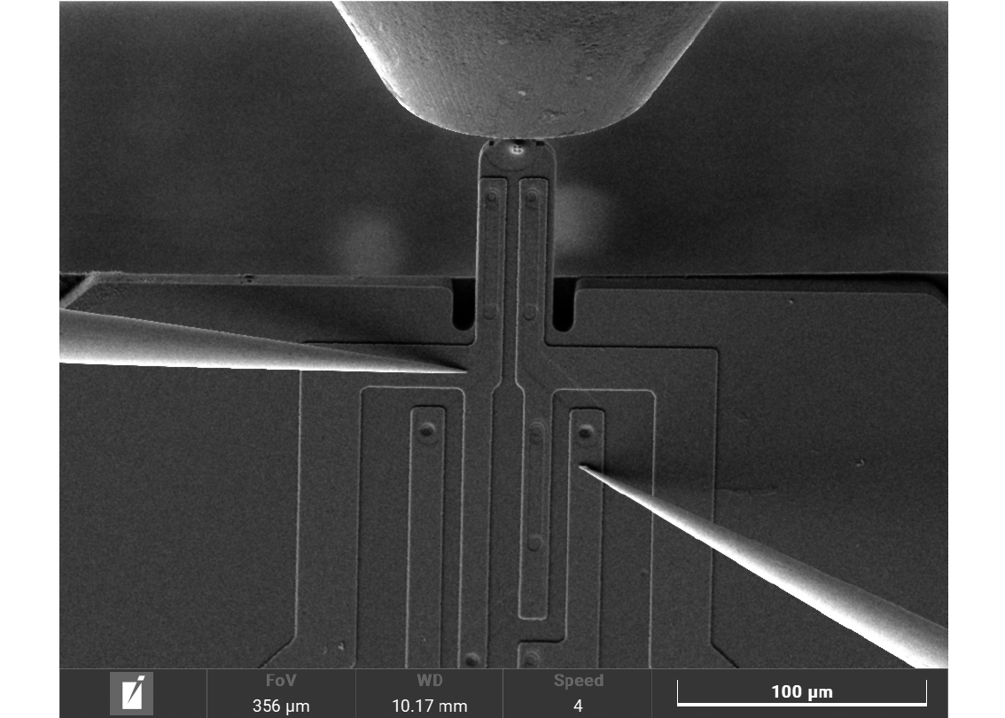
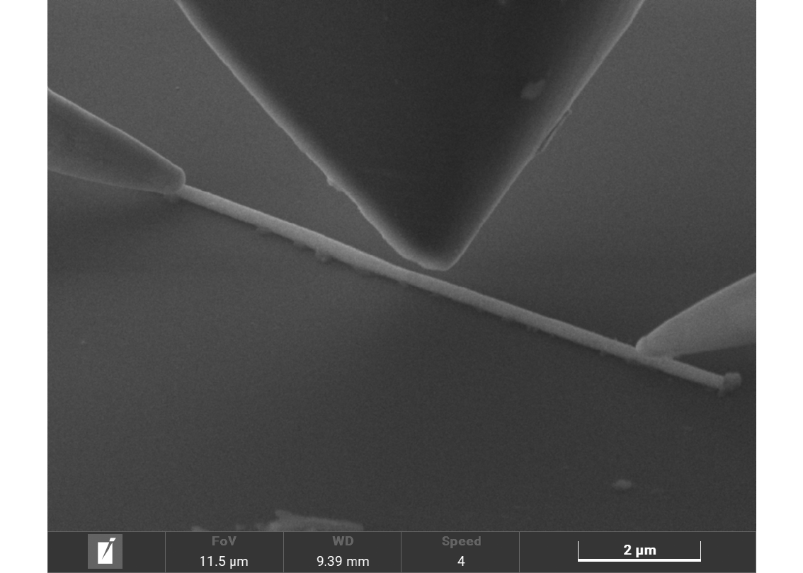
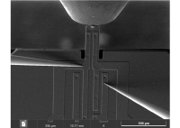
In this proof-of-principle application note, we show a deformation of an actuated piezoresistive AFM cantilever, and a change of electrical current passing through a deformed PtCr metal line, as examples of such combined electrical/mechanical in-situ analysis.
The integrated solution is straightforward to use and easy to learn. It is aimed to enhance our understanding of microscale phenomena and to help design safer electronic applications.
There are several application areas, where this combined approach would be highly beneficial:
Advanced AFM with simultaneous electrical probing
Electrical microprobing combined with nanoindentation
Our solutions are distributed worldwide through our network of qualified partners. We are here to support you! Get in touch with us, we are committed to assist you in selecting the products that best meets your needs.