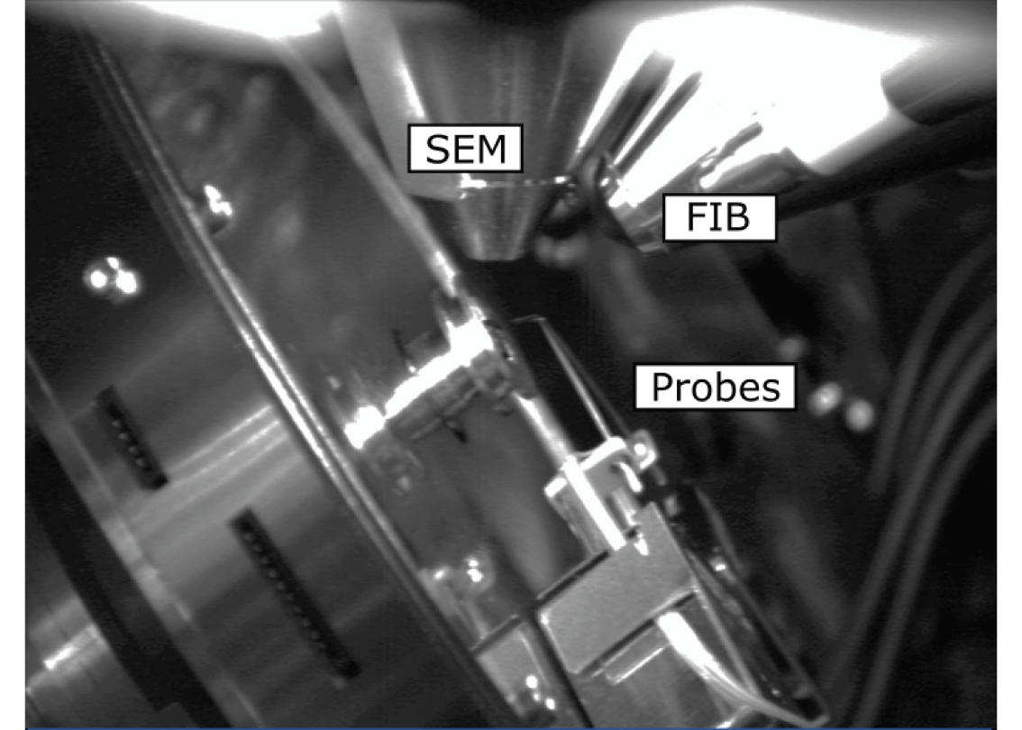
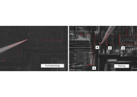
In the field of semiconductor failure analysis, the use of Electron Beam Absorbed Current (EBAC) combined with FIB-cut in Dual Beams has become popular to investigate shorts and opens between metal lines.
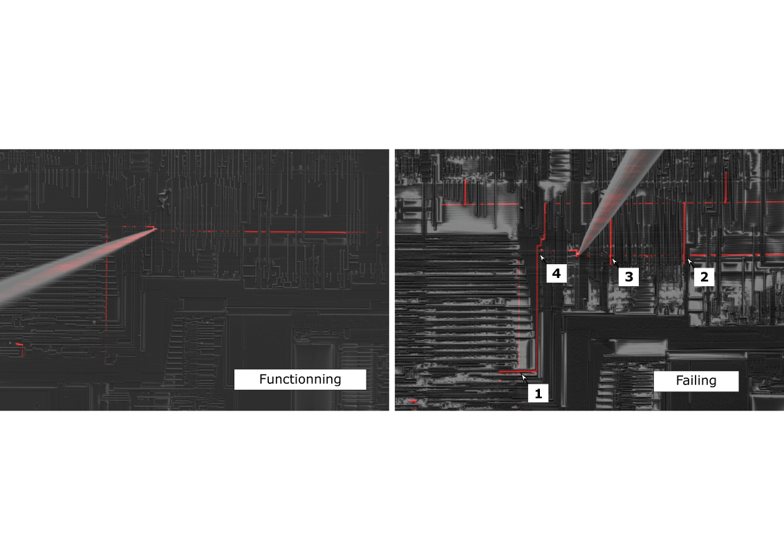
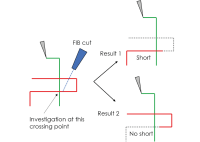
In this article, we describe the defect localization of a short between two networks on an ASIC from the automotive industry. These networks are crossing each other at four different locations.
We used a combination of FIB-cuts with EBAC images to determine the crossing point where the short is located, with the following procedure:
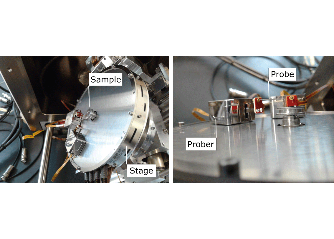
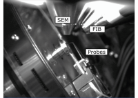
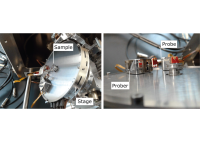
This application shows the ability of the miBot™ nanoprobers to precisely position and land probes when the microscope sample stage is tilted.
Fraunhofer CAM, Halle, Germany
W. Courbat and J. Jatzkowski,“Faster and More Accurate Failure Analysis: Circuit Editing and Short Localization Performed at Same FEB Tilt Angle using Multiple Techniques”, Electronic Device Failure Analysis, 21(4), p. 22-28, 2019.
Electrical failure analysis and semiconductor defect localization techniques
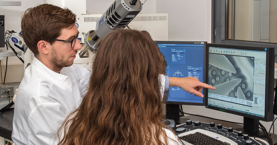
We have fully equipped demo lab for semiconductor electrical failure analysis. Our applications team is eager to perform live demonstrations and feasibility studies for you, onsite or online.
In the meantime, do not miss the opportunity to learn more about our products and applications with one of our webinars!