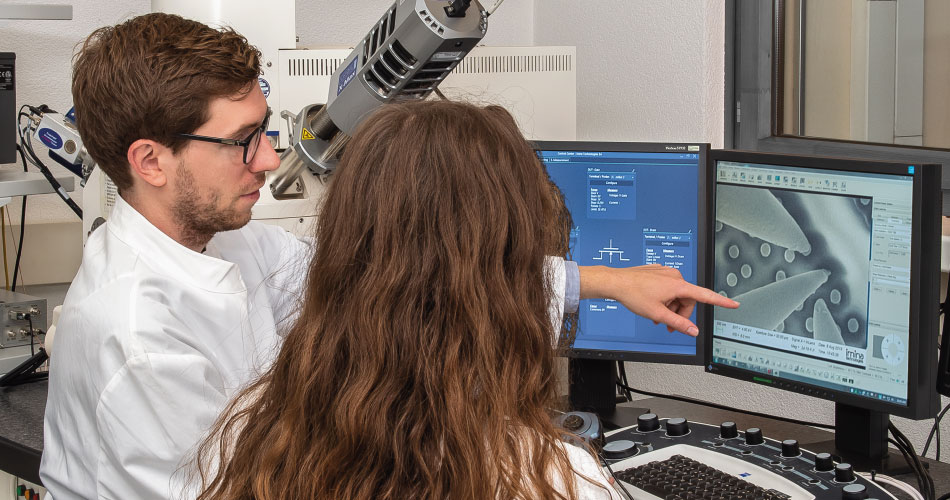
Electron Beam Induced Current (EBIC) and Electron Beam Absorbed Current (EBAC), also called Resistive Contrast Imaging (RCI), are two techniques used to locate and analyze failures inside semiconductor devices. Both methods take advantage of the interaction of the electron beam of the scanning electron microscope (SEM) with the device under test (DUT) to reveal information to the failure analysis investigator.
EBIC provides the means to visualize and quantitatively determine properties like the diffusion length of transistor p-n junctions. With Imina Technologies' nanoprobing solutions, probe needles are placed in contact with a junction to measure the induced current. The EBIC system amplifies the point probe measurements and synchronizes them to the electron beam position. This information can then be mapped and overlaid to the microscope secondary electron image with the EBIC system for visualization.
The EBAC technique is based on a similar principle to EBIC. The SEM's electron beam scans the DUT and injects charges absorbed by metal lines below the surface. A current is then induced and measured by a probe placed with a miBot nanomanipulator at the contact level. As with the EBIC technique, the probed signal can be superimposed on the secondary electron image. The comparison of this image with the circuit layout allows the investigator to precisely locate the shorts and opens.
Fraunhofer CAM, Halle, Germany
Defect localization at transistor gate using electron beam induced resistance change (EBIRCh)
Electrical failure analysis and semiconductor defect localization techniques
We have fully equipped demo lab for semiconductor electrical failure analysis. Our applications team is eager to perform live demonstrations and feasibility studies for you, onsite or online.
In the meantime, do not miss the opportunity to learn more about our products and applications with one of our webinars!
