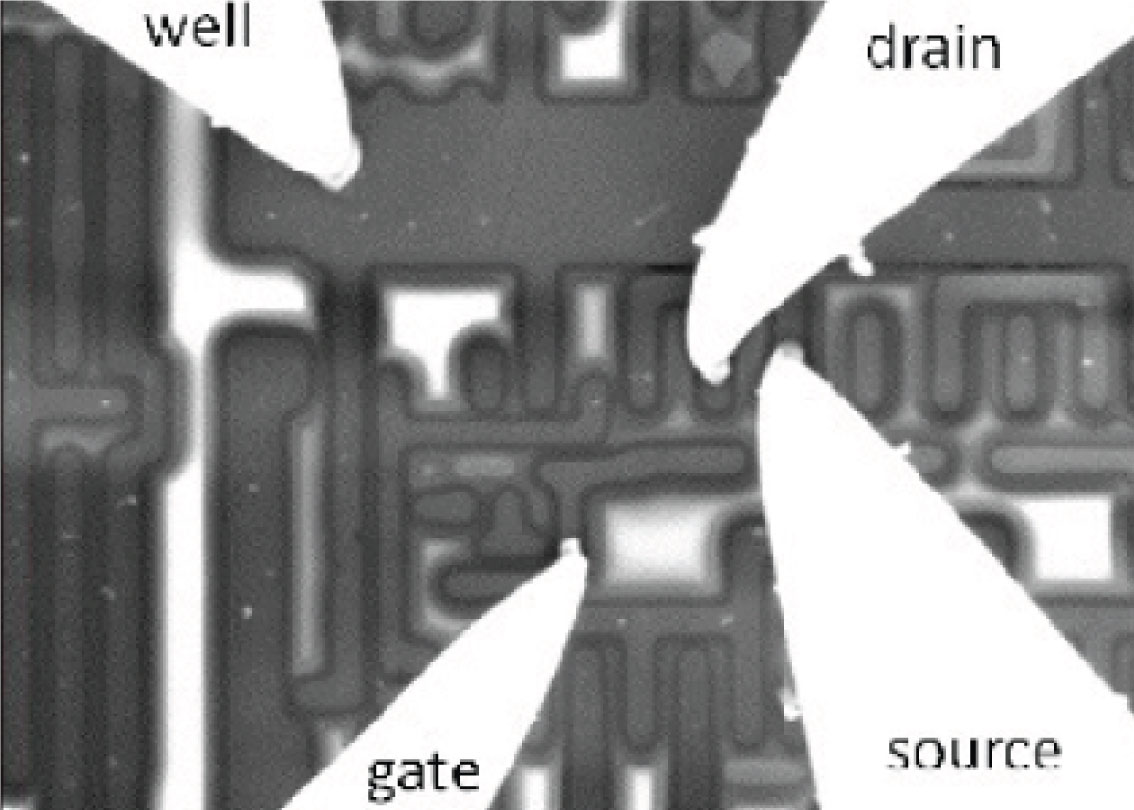
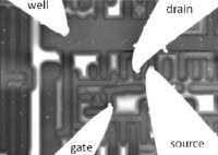
Transistor nodes size has kept decreasing down to a few tenths of nanometers. This makes the characterization of a single transistor impossible to carry out under a conventional probe station.
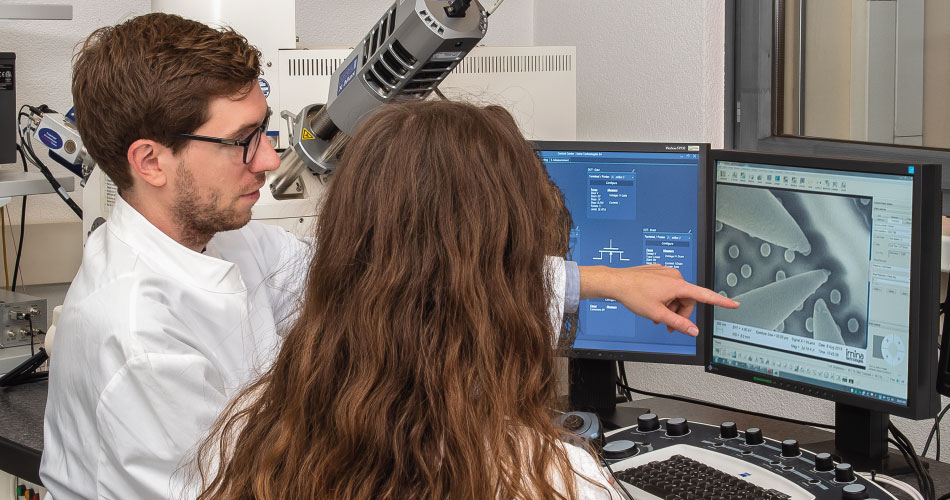
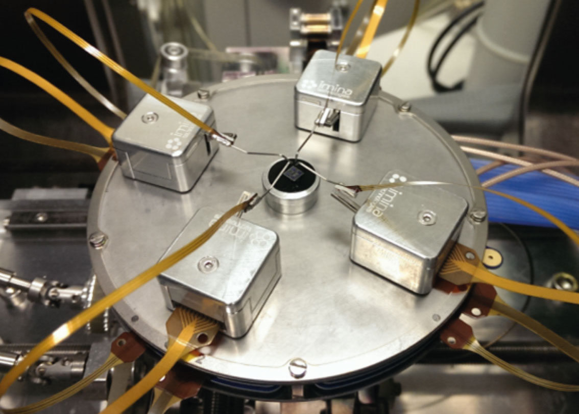
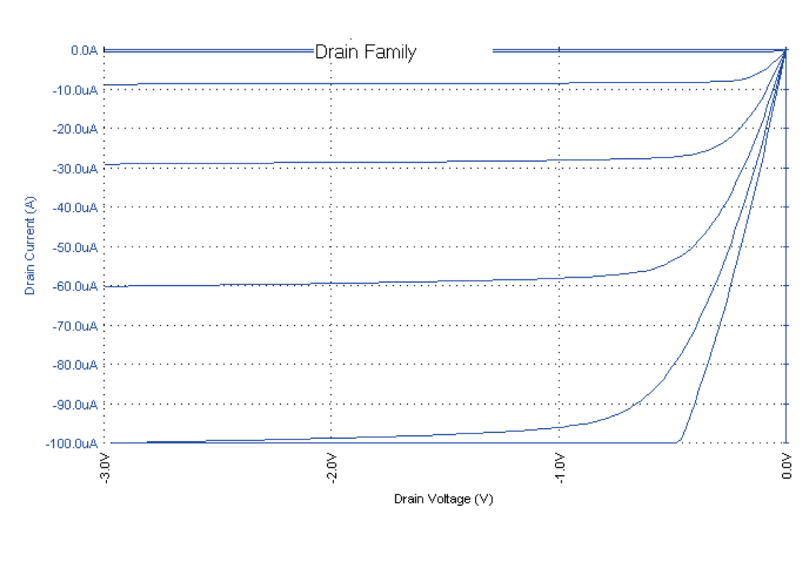
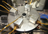
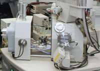
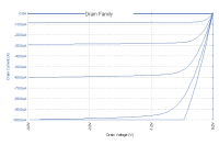
This application note reports on the characterization of PMOS field-effect transistors inside the SEM by means of nanoprobers. Imina Technologies Nanoprobing SEM solution loaded with four miBot™ nanomanipulators enables the investigator to precisely put down probes directly on metal lines. Electrical measurements are performed with a Keithley 4200-SCS semiconductor parameter analyzer.
The unique mobile motion technology of the micro-robots allows the operator to adjust the probe orientation in real-time to adjust to the geometry of the device under test. This avoids to have to open the microscope vacuum chamber, significantly accelerating the process throughput.
We have fully equipped demo lab for semiconductor electrical failure analysis. Our applications team is eager to perform live demonstrations and feasibility studies for you, onsite or online.
In the meantime, do not miss the opportunity to learn more about our products and applications with one of our webinars!