Electron beam current collection techniques (EBIC/EBAC/EBIRCH) are widely used in electrical failure analysis to localize defects either by highlighting the defect’s location in the electrical current image or by juxtaposition of a reference and a failing sample.
Signal calibration can take these techniques to another level. In our new application note, we use calibrated EBIC signal acquisition to measure the minority charge carrier diffusion length at the p-n junction of a GaAs solar cell.
Minority charge carriers are either electrons or holes depending on the semiconductor doping. Their diffusion length, or lifetime, is related to defects or dislocation density in a semiconductor, and therefore can serve as a metric to evaluate the semiconductor quality.
Experiment details
We used Imina Technologies’ Nanoprobing system equipped with Point Electronic’s EFA module to measure the diffusion length of minority carriers in a solar cell.
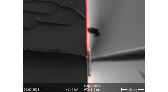
The EBIC signal was collected from the solar cell cross-section containing a p-n junction.
miBot nanoprobers are so mechanically stable that the microscope stage could be tilted back and forth without losing electrical contact, which tremendously helped to streamline the experiment workflow and get results quickly.
Well-calibrated Point Electronic’s EBIC signal acquisition module provided accurate pixel current values for all amplification configurations, so we could quantify the device characteristics.
Results
We collected 50 line-profiles of the EBIC signal and used them to calculate the diffusion length of minority charge carriers, which amounted to 570 nm, which is within the expected range for such devices. We also estimated that the surface recombination velocity is close to zero, which suggests a low density of defects in the semiconductor layer of the solar cell.
Quantitative EBIC can be a powerful complementary tool to the regular EBIC and to quickly provide insight into the local properties of semiconductors. With the raising complexity of semiconductor devices, having a way to gain more quantitative data about devices following a customary workflow, can save a lot of time and effort while troubleshooting or optimizing the IC design.
Read the full application note here.
References
[1] G. Moldovan, The emergence of electrical analysis in electron microscopy, Microscopy and Analysis, 2020.
[2] D. Chan, V. Ong, A direct method for the extraction of diffusion length and surface recombination velocity from an EBIC line scan, IEEE transactions on electron devices, 1995.