Electron beam current collection techniques (EBIC/EBAC/EBIRCH) are widely used in electrical failure analysis to localize defects. These techniques either produce a spot highlighting the defect’s location in the electrical current image or serve for a comparison of a reference and a failing sample. Some defects, damages or process variations require quantitative analysis of current values measured at each pixel. It is especially true for the electron beam induced current (EBIC). From EBIC signals, one can quantify carrier mobility, diffusion lengths, recombination processes, and defect distribution within the material. This information is crucial for understanding the performance and quality of semiconductor devices, which, in turn, leads to improved design and fabrication processes.
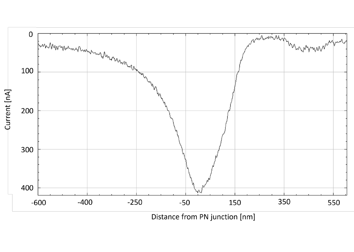
In order to obtain specific parameters describing the charge carrier dynamics, one needs to associate accurate current values with each pixel of the EBIC image. In this application note, we show how calibrated EBIC signal acquisition can be used to measure the minority charge carrier diffusion length at the p-n junction of a GaAs solar cell. Minority charge carriers are either electrons or holes depending on the semiconductor doping. Their diffusion length, or lifetime, is related to defects or dislocation density in a semiconductor.
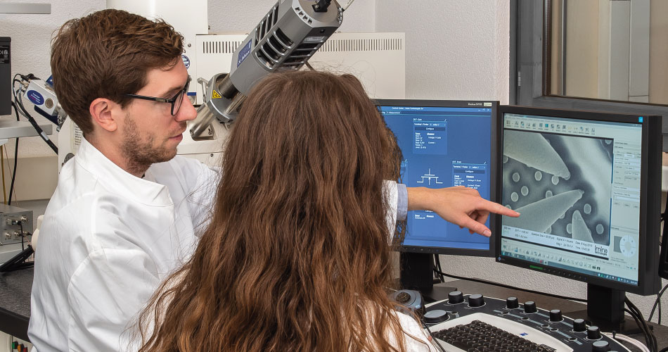
In this Application note, we used Imina Technologies’ Nanoprobing system equipped with Point Electronic’s EFA module to measure the diffusion length of minority carriers in a solar cell.
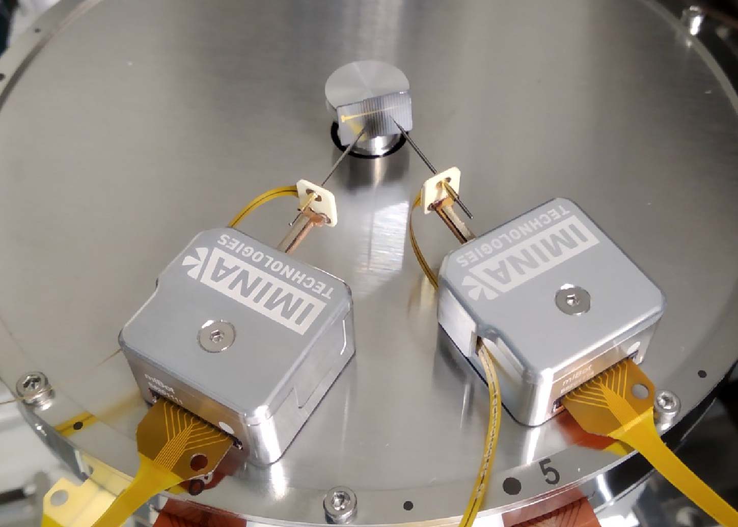
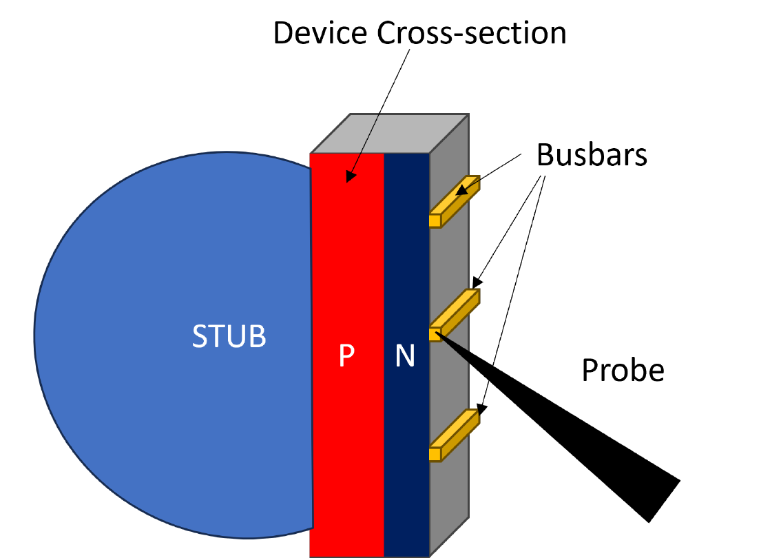
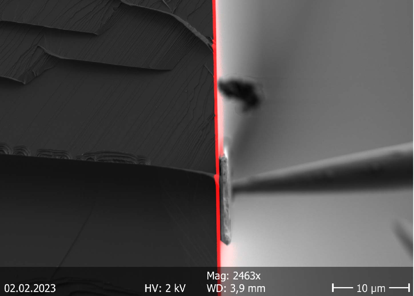
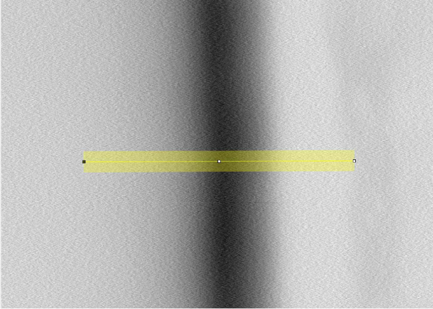
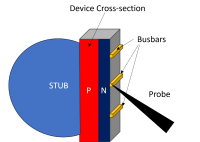
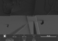
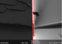
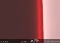
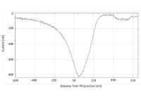
We collected EBIC signal from the solar cell cross-section containing a p-n junction.
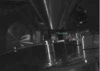
miBot nanoprobers are so mechanically stable that the microscope stage could be tilted back and forth without losing electrical contact, which tremendously helped to streamline the experiment workflow and get results quickly and efficiently.
Thanks to the well-calibrated Point Electronic’s EBIC signal acquisition module, we obtained accurate pixel current values for all amplification configurations and could quantify the device characteristics.
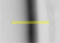
We collected 50 line-profiles of the EBIC signal and used them to calculate the diffusion length of minority charge carriers, which amounted to 570 nm, which is within the expected range for such devices. We also estimated that the surface recombination velocity is close to zero, which suggests a low density of defects in the semiconductor layer of the solar cell.
[1] G. Moldovan, The emergence of electrical analysis in electron microscopy, Microscopy and Analysis, 2020.
[2] D. Chan, V. Ong, A direct method for the extraction of diffusion length and surface recombination velocity from an EBIC line scan, IEEE transactions on electron devices, 1995.
Cross-section EBIC of a transistor array using a Large Sample Adapter
Metal layers short localization with EBAC and FIB circuit modifications performed at 54° stage tilt
Defect localization at transistor gate using electron beam induced resistance change (EBIRCh)
We have fully equipped demo lab for semiconductor electrical failure analysis. Our applications team is eager to perform live demonstrations and feasibility studies for you, onsite or online.
In the meantime, do not miss the opportunity to learn more about our products and applications with one of our webinars!