Semiconductor devices are typically designed to operate between 0 and 70°C, which is considered the normal operating temperature range. Sometimes though, devices get to work at lower or higher temperatures. Away from the normal operating temperature range, devices may consume more power, leak current or crack due to the thermal expansion, and overall be less reliable in the long-term. Specific behavior of transistors at different temperatures can vary depending on the transistor technology, design, and the materials used. Testing thermal behavior of a given device is an important part of quality assurance and risk management.
Our thermal stage for in-situ SEM nanoprobing covers temperature range from -30°C to 150°C. This range corresponds to the practical extension of normal operation conditions for semiconductor devices or can be used for accelerated testing to predict the lifetime of a device in normal conditions from its behavior at 150°C.
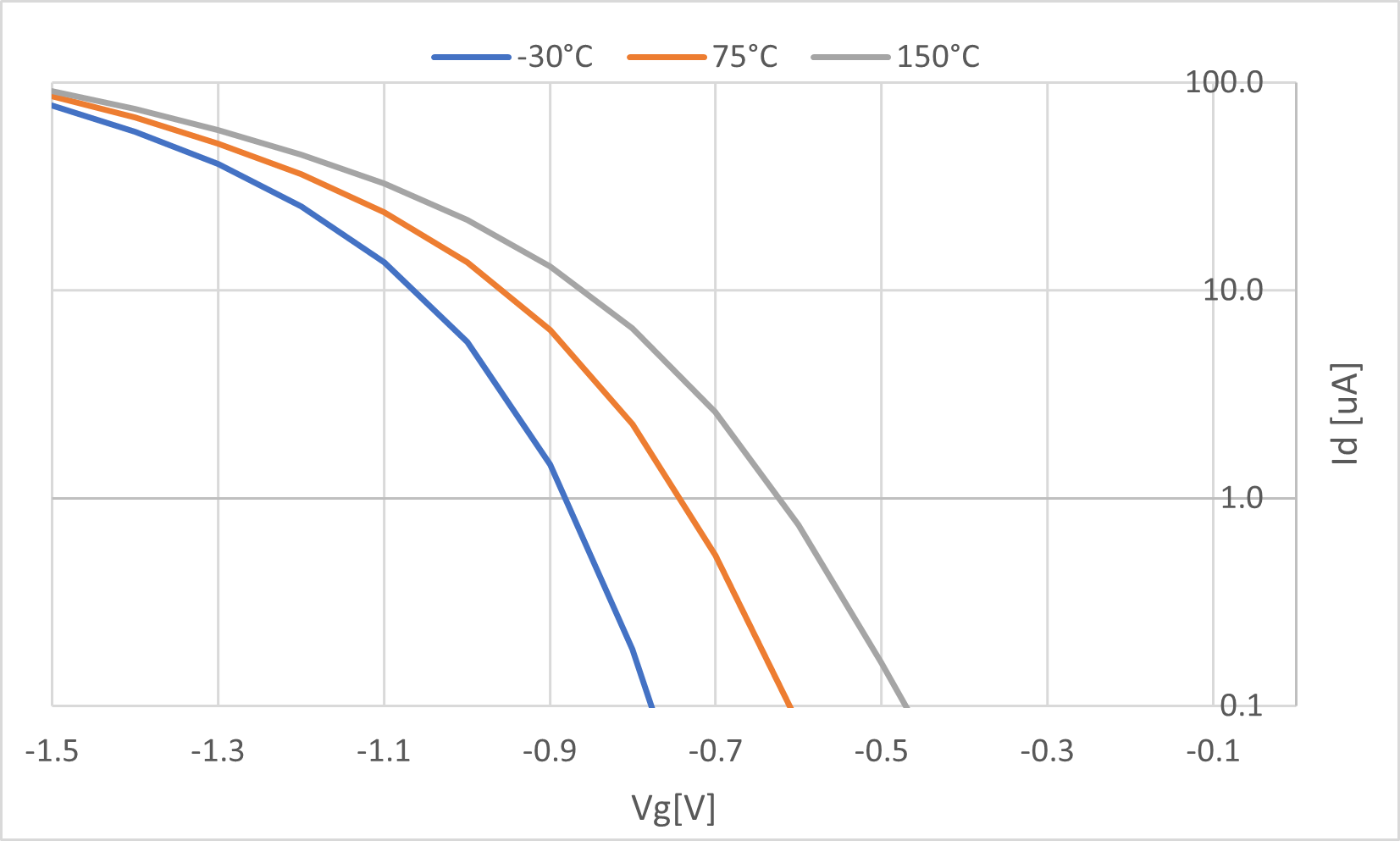
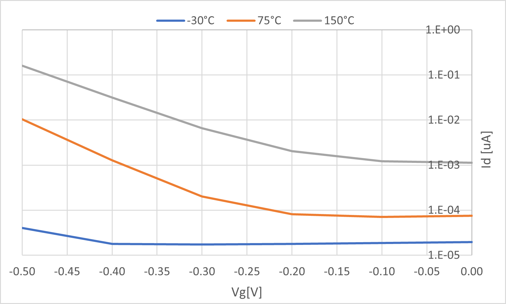
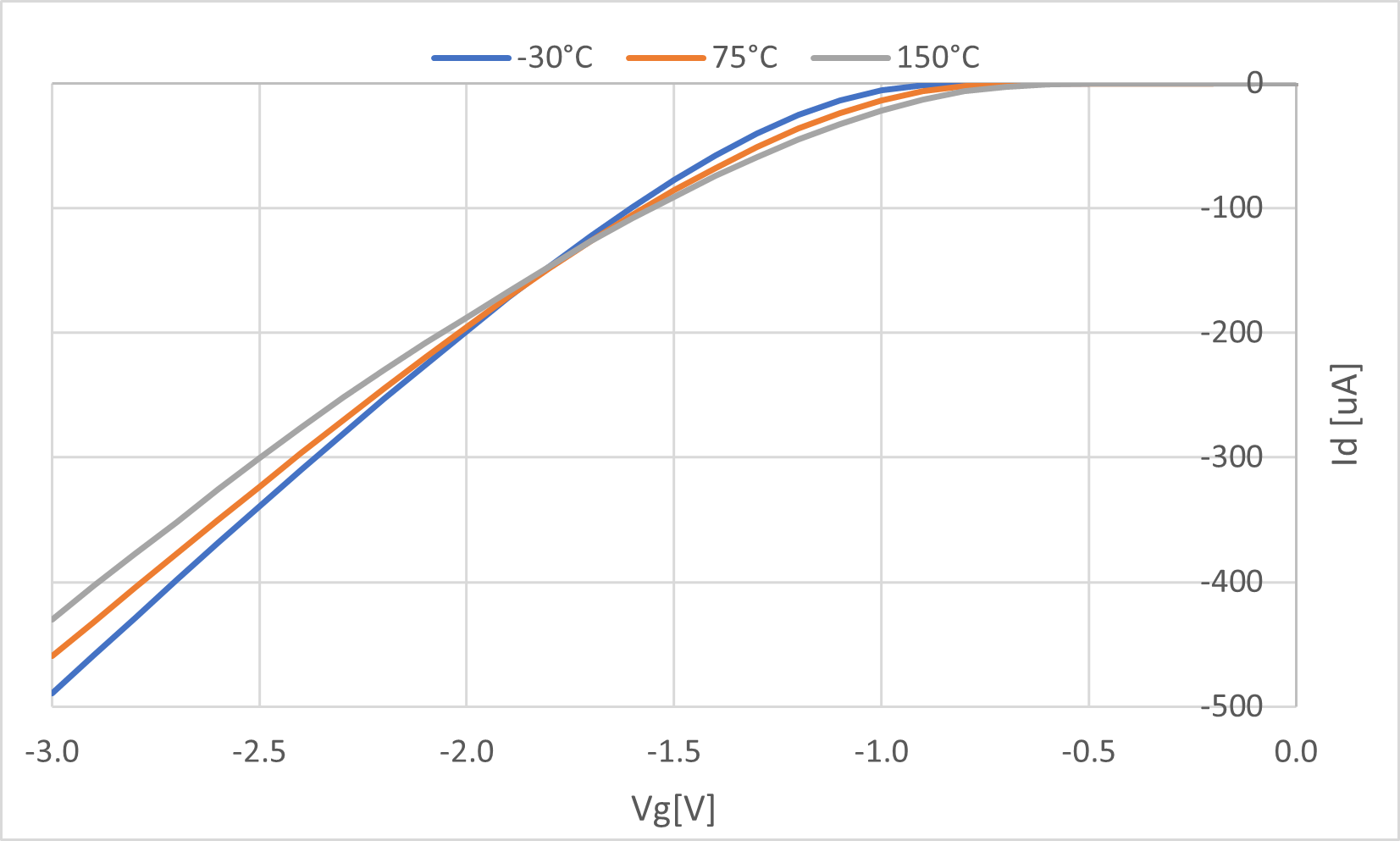
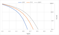
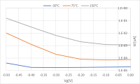
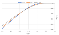
At high temperature, we expect a decrease in threshold voltage (the voltage at which the transistor starts conducting) and drain current at saturation (current that flows between the drain and source terminals when transistor is on) and an increase in off-current (current that flows between the drain and source terminals when transistor is off).
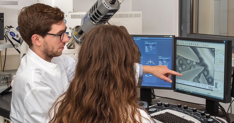
In this application note, we tested thermal behavior of a PMOS transistor of 180 nm technology node. The transistor has been delayered to contact level and loaded into TESCAN Clara SEM equipped with Imina technologies’ NANO system with a thermal stage. We analyzed how threshold voltage, drain current at saturation and off-current behave at -30, 75 and 150°C.
We observed the expected decrease in threshold voltage and current at saturation, and a decrease in off-current, which suggests higher leakage.
With our thermal stage, such measurements can be done in-situ SEM, and the users can enjoy freedom of movement around the platform, and easy and precise probe landing of miBot nanoprobers while testing their samples at different temperatures.
Thermal stage is an optional module for Imina Technologies’ NANO 8-bot system. Existing setups can be upgraded with the thermal stage, as long as Precisio software is updated to the latest version that includes the thermal stage control module.
Contact us if you are interested in our thermal stage, or if you would like to incorporate thermal sample analysis in the nanoprobing service.
Defect localization at transistor gate using electron beam induced resistance change (EBIRCh)
We have fully equipped demo lab for semiconductor electrical failure analysis. Our applications team is eager to perform live demonstrations and feasibility studies for you, onsite or online.
In the meantime, do not miss the opportunity to learn more about our products and applications with one of our webinars!