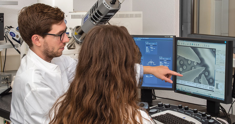
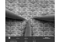
The components of integrated circuits (IC) are getting smaller and smaller. To keep up with this trend, IC design engineers increasingly rely on in-situ scanning electron microscope (SEM) nanoprobing. It serves to characterize the performance of microchips and to find faulty components, helping to optimize the IC design.
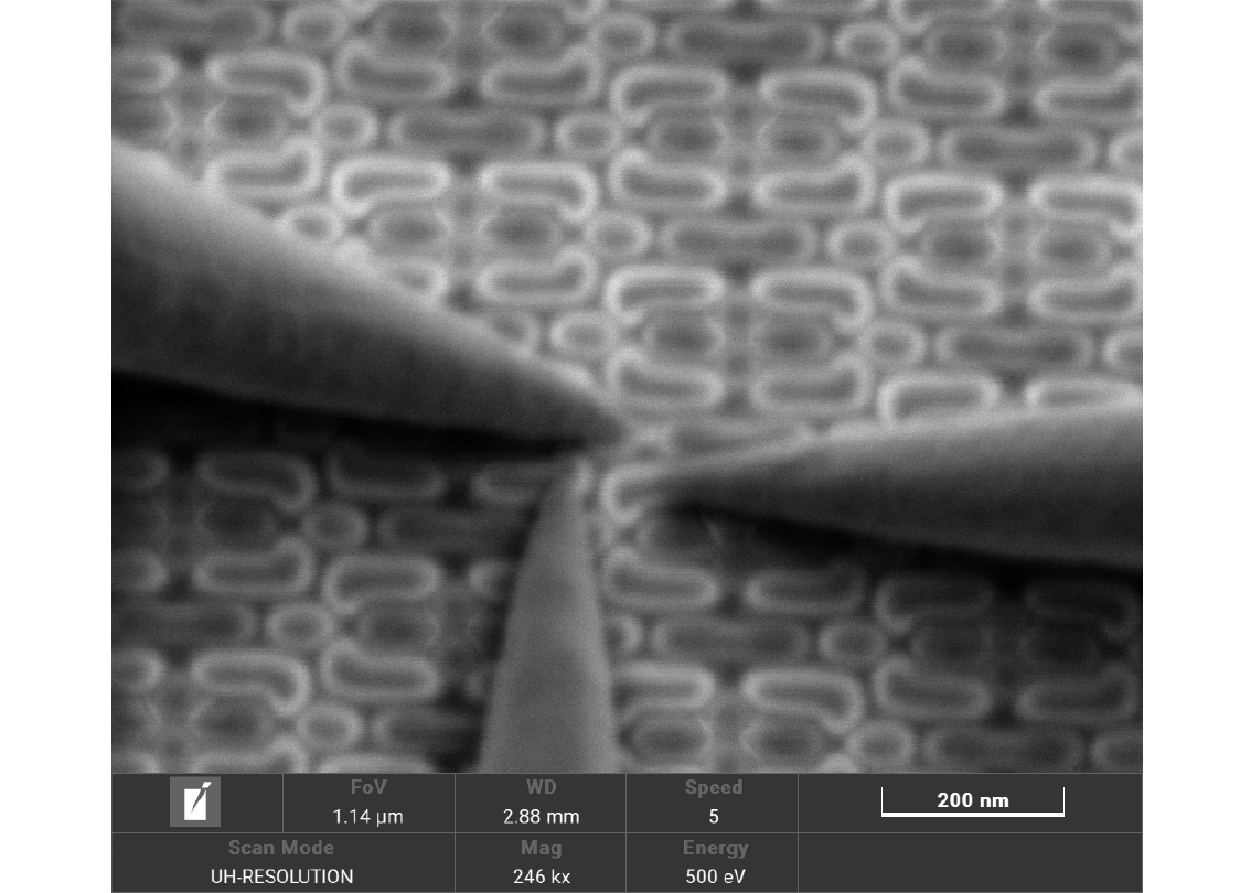
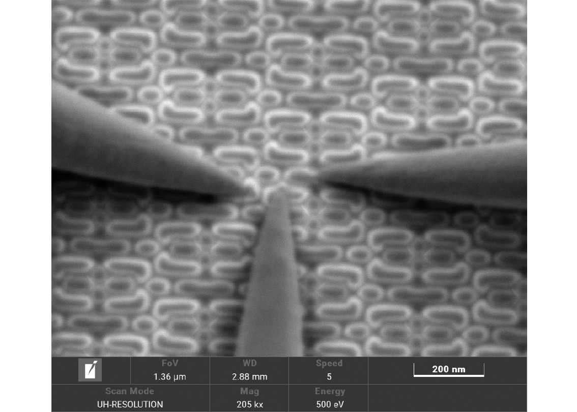
In this application note, we show how Imina Technologies’ Nanoprobing Solution can be used to characterize NMOS and PMOS transistors of a 5 nm technology node chip inside the TESCAN Clara SEM.
The Nanoprobing Solutions from Imina Technologies provide excellent signal-to-noise ratio and optimized workflow for transistor characterization, which are crucial for working with few-nm node technologies. Such small nodes are tricky to image because SEM should operate under low acceleration voltage and at short working distance. Electrical characterization is also challenging because the probes have to be precisely positioned and to maintain a stable electrical contact with the sample during the whole experiment. Imina Technologies’ Nanoprobing Solution is designed to perform reliable measurements on such small nodes. It also offers optimized workflow and significantly reduced time-to-data.
Electrical nanoprobing of NMOS and PMOS transistors on 22, 14, and 10 nm semiconductor devices
Defect localization at transistor gate using electron beam induced resistance change (EBIRCh)
Failure mechanism investigation of single bits in flash memory array
EBIC / EBAC techniques for semiconductor failure analysis
We have fully equipped demo lab for semiconductor electrical failure analysis. Our applications team is eager to perform live demonstrations and feasibility studies for you, onsite or online.
In the meantime, do not miss the opportunity to learn more about our products and applications with one of our webinars!